

技术前沿:半导体先进封装从2D到3D的关键
描述
技术前沿:半导体先进封装从2D到3D的关键
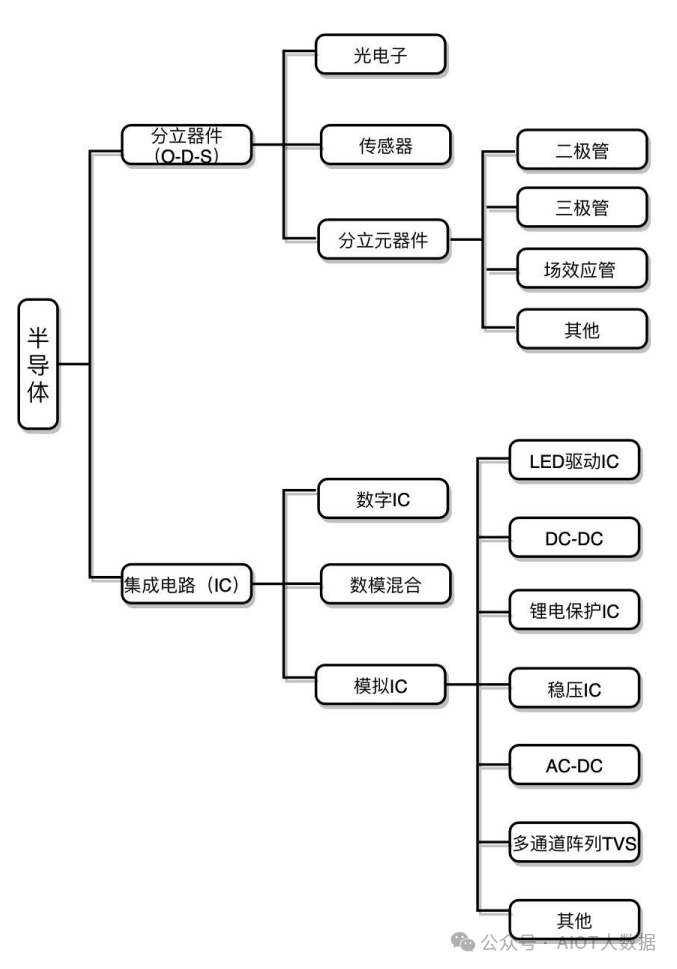
半导体分类
集成威廉希尔官方网站 封测技术水平及特点
1. 发展概述
·自20世纪90年代以来,集成威廉希尔官方网站 封装技术快速发展,推动了电子产品向小型化和多功能方向迈进。
·随着芯片结构需求的变化,封装技术逐步从单项技术或混合应用技术发展为高级封装技术,以适应下游领域的需求。
2. 按照封装结构分类的技术演进
·发展历程:
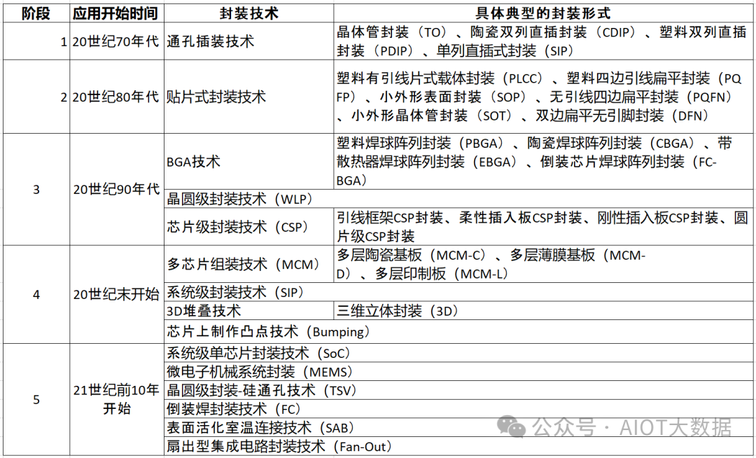
金属圆形封装(TO) → 双列直插封装(DIP) → 塑料有引线片式载体(PLCC) → 四边引线扁平封装(QFP) → 针栅阵列(PGA) → 球栅阵列(BGA) → 芯片尺寸封装(CSP) → 多芯片组件(MCM) → 系统级封装(SIP)
·技术特点:
oDIP(双列直插封装):
§通用型插装封装,引脚从两侧引出。
§常用于传统集成威廉希尔官方网站 ,结构简单,适合通孔安装。
oPQFP(塑料方块平面封装):
§引脚间距小,管脚细。
§适用于大规模或超大规模集成威廉希尔官方网站 (引脚数超过100)的封装。
oTQFP(薄塑封四角扁平封装):
§节省空间,减小体积和高度。
§适用于对散热要求较高的集成威廉希尔官方网站 产品。
3. 按照连接方式分类的技术演进
·引线键合(WB) → 载带自动键合(TAB) → 倒装芯片键合(Flip Chip) → 硅通孔(TSV)。
4. 按照装配方式分类的技术演进
·通孔插装(THT) → 表面组装(SMT) → 直接安装(DCA)。
5. 传统封装与先进封装
·传统封装:
o代表技术:DIP、SOT、SOP等。
o优势:成熟工艺,成本较低。
o劣势:体积较大,性能受限。
·先进封装:
o技术路径:
1.晶圆级芯片封装(WLCSP):
§扇入型封装(Fan-In):适合单芯片小体积应用。
§扇出型封装(Fan-Out):引脚密度高,性能提升。
§倒装(Flip Chip):提高电气性能,适合高频应用。
2.系统级封装(SIP):
§将多个裸片封装在一起,集成不同功能模块。
§提高集成度,适用于复杂系统需求。
·先进封装的优势:
o更高的性能、更低的功耗。
o满足现代电子产品的高集成化和多功能需求。
6. 国内封测行业现状
·国内一流封测厂商已掌握多项先进封装技术。
·中小规模厂商在传统封装技术基础上,不断投入研发资源,探索先进封装技术。
·未来发展方向:重点研发晶圆级封装与系统级封装。
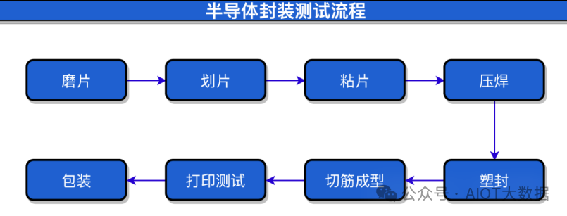
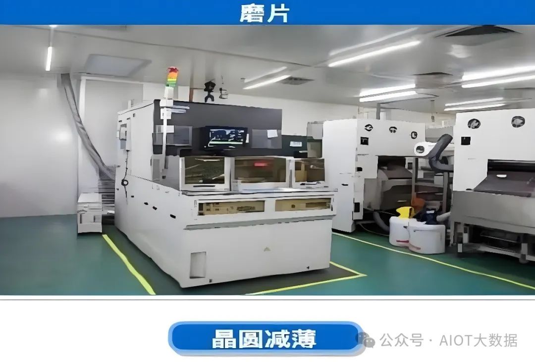
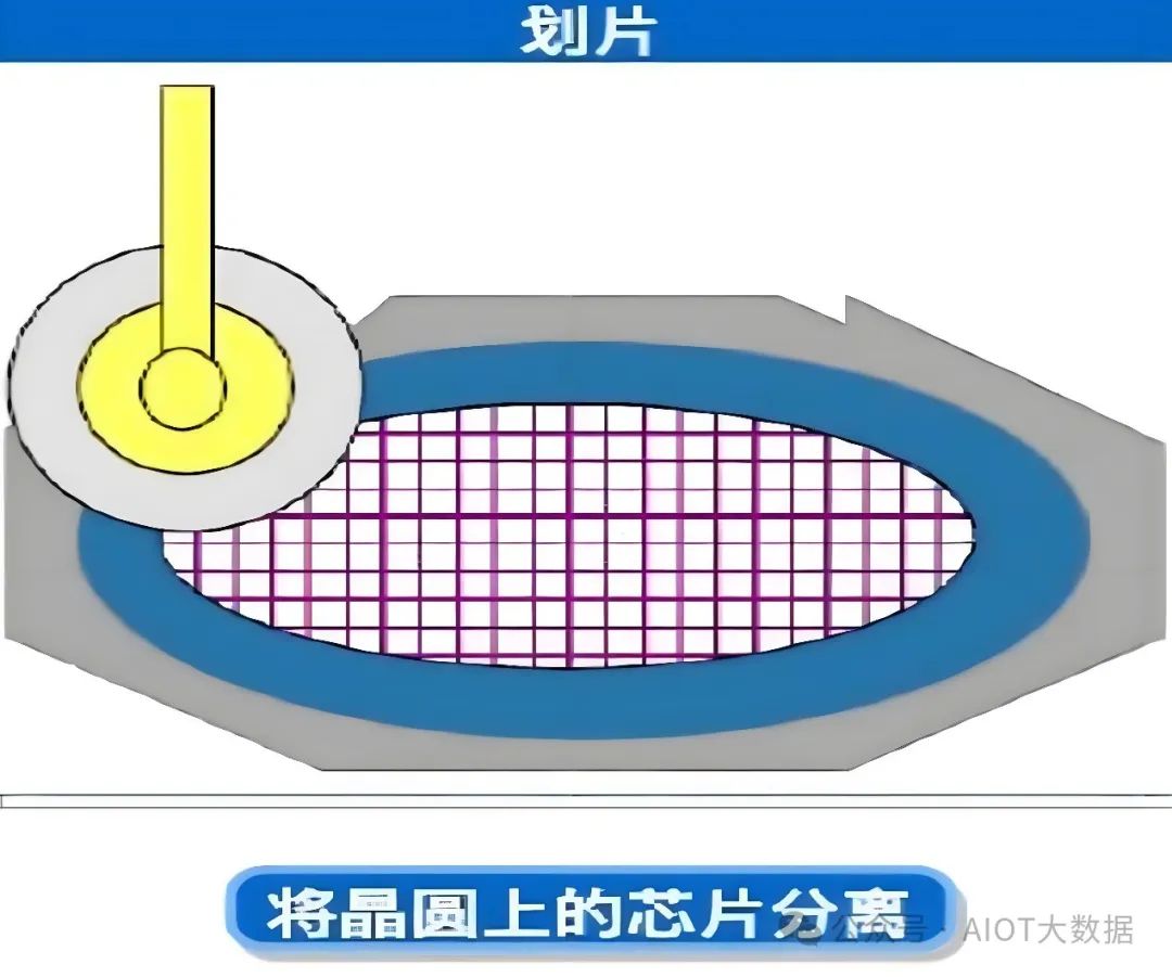
半导体封装测试流程
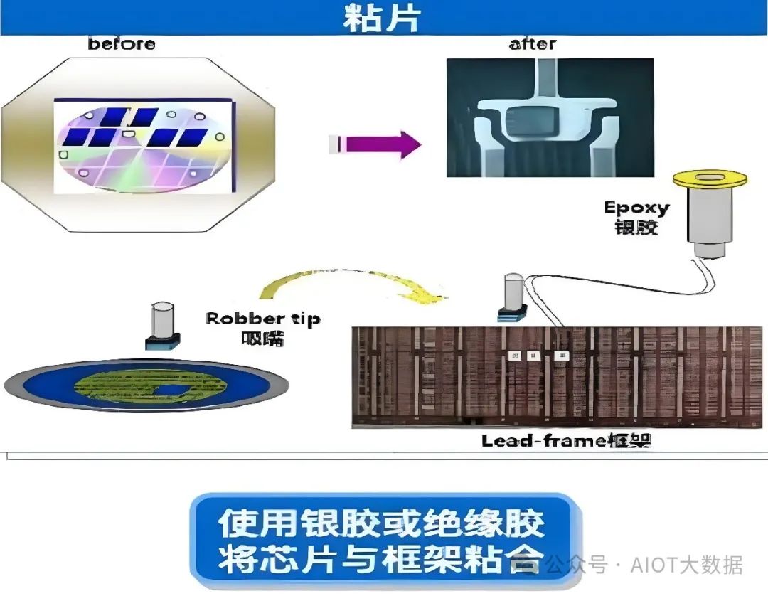
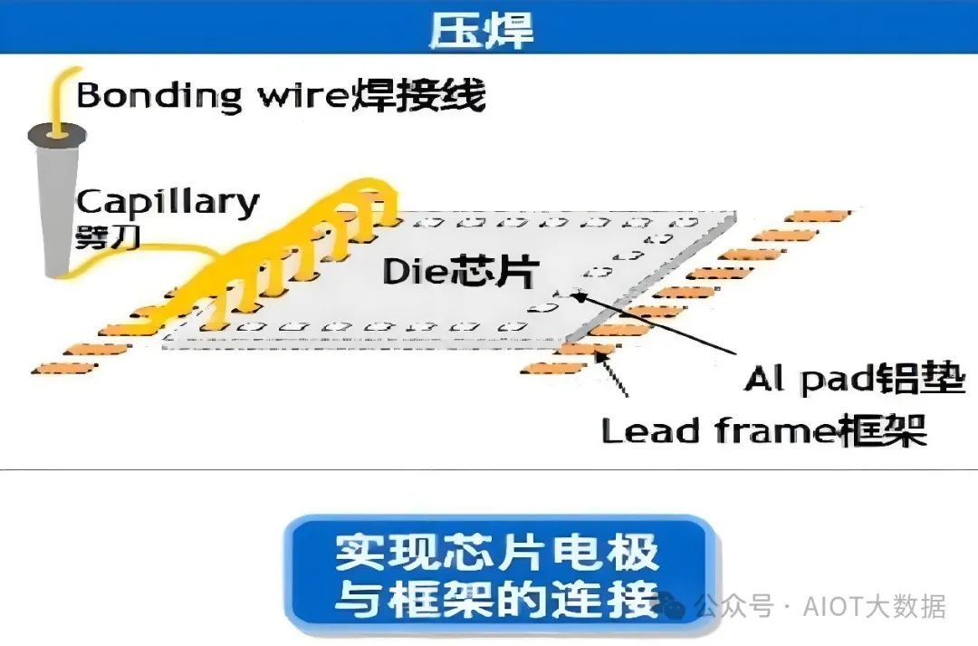
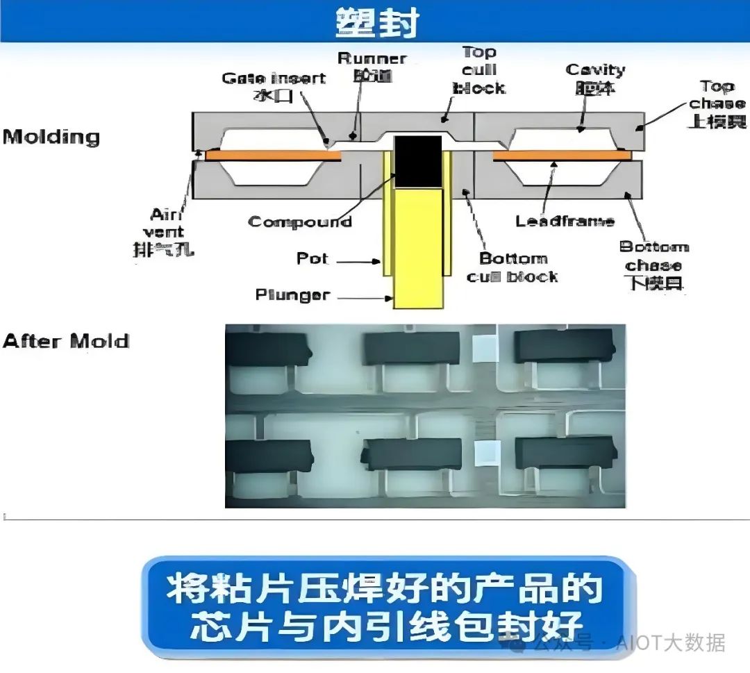
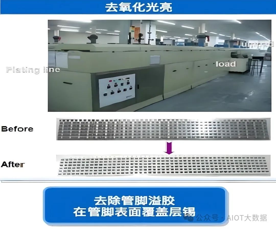
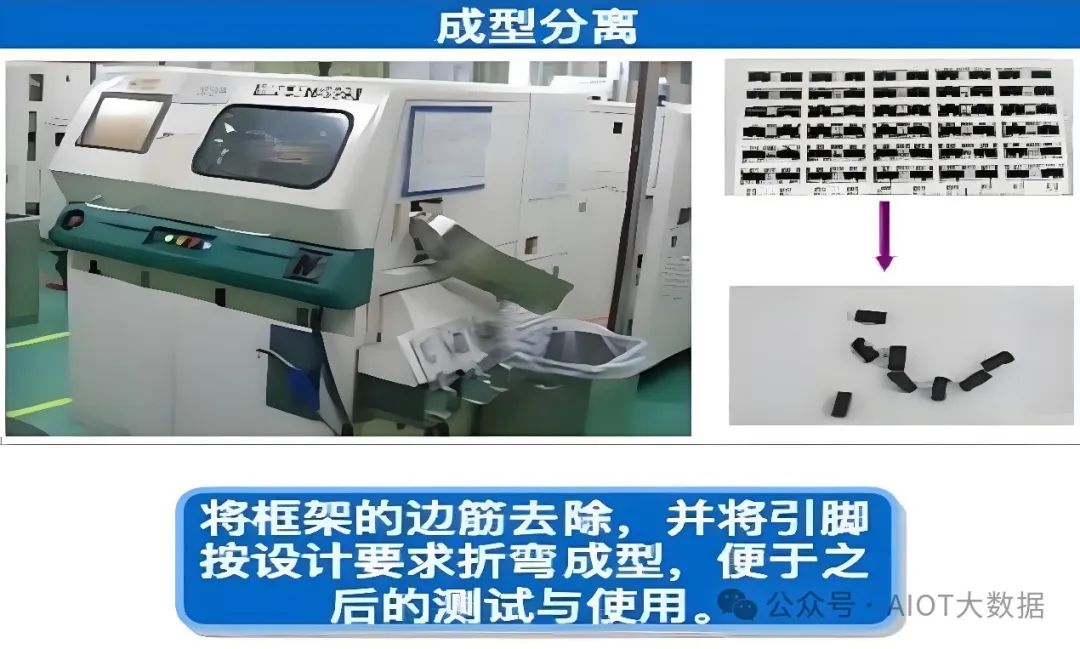
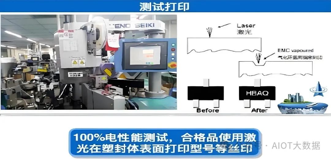
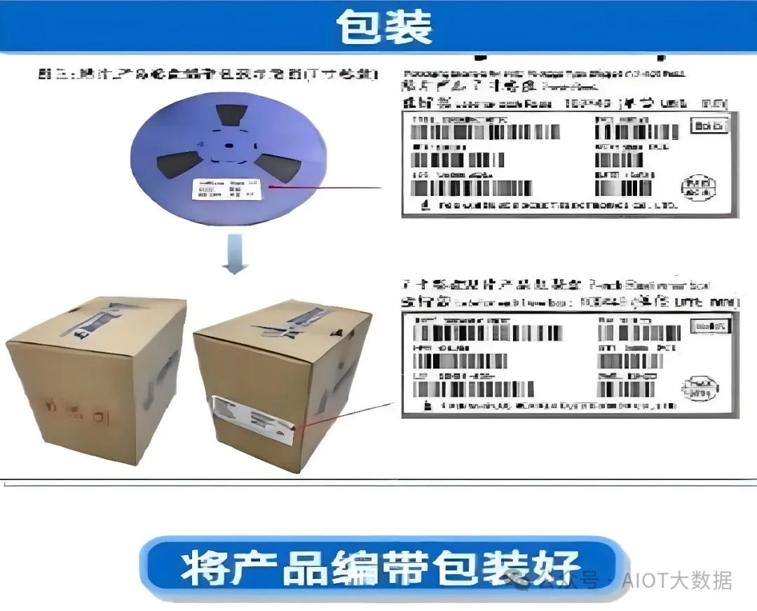
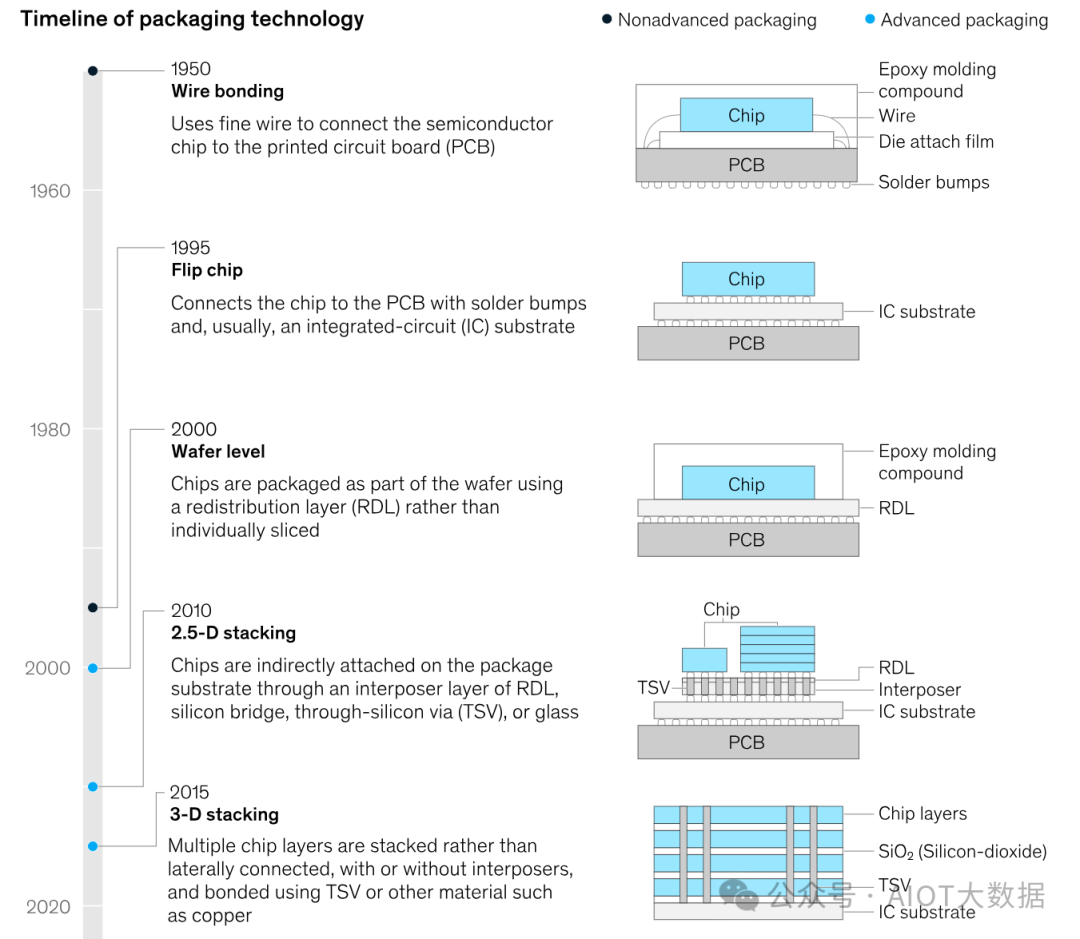
半导体封测发展历史
A Comprehensive Comparison of IC Packaging Interconnect Technologies
IC封装互连技术综合比较
INTRODUCTION 介绍
When it comes to IC package interconnect selection, design engineers need to factor-in a host of complex issues, including cost, performance, end-use applications and much more. Two predominant technologies, Flip Chip and Wire Bonding, are popular interconnect options connecting ICs to packages or substrates.
在选择IC 封装互连时,设计工程师需要考虑许多复杂的问题,包括成本、性能、最终用途应用等。倒装芯片和引线键合这两种主要技术是将 IC 连接到封装或基板的流行互连选项。
Both bonding techniques play a crucial role in the fabrication and performance of electronic devices, while each presents its own unique advantages and challenges. This article compares in detail many critical factors influencing the selection of the optimal IC package interconnect option as it relates to a variety of different performance requirements.
这两种键合技术在电子设备的制造和性能中都发挥着至关重要的作用,同时每种技术都有其独特的优势和挑战。本文详细比较了影响最佳 IC 封装互连选项选择的许多关键因素,因为它涉及各种不同的性能要求。
MAIN CHARACTERISTICS: 主要特点:
| Feature 特征 | Wire Bonding 打线键合 | Flip Chip 倒装芯片 |
|
General Description 一般说明 |
Wire Bonding is a long-standing and popular interconnection method, that uses thin metallic bond wires, typically made of gold, aluminum or copper, that are thermally or ultrasonically connected to chip terminals on one end, and the package pins or PCB on the other end. 引线键合是一种长期流行的互连方法,它使用细金属键合线,通常由金、铝或铜制成,一端通过热或超声波连接到芯片端子,另一端连接到封装引脚或PCB结尾。 |
Flip Chip, AKA Controlled Collapse Chip Connection (C4), is an advanced packaging technology whereby the chip is flipped upside-down and connected directly to the substrate using small solder bumps. Bumps serve as electrical and mechanical connections between the chip and the substrate. 倒装芯片,又称受控塌陷芯片连接 (C4),是一种先进的封装技术,将芯片上下翻转并使用小焊料凸块直接连接到基板。凸块充当芯片和基板之间的电气和机械连接。 |
| Bonding Types 粘合类型 |
Two main types of Wire Bonding: 引线键合的两种主要类型: · Ball Bonding: Process typically uses gold wire. A small ball is formed at the end of the wire and attached to the bond pad using heat and pressure. The other end of the wire is then connected to the chip package using ultrasonic energy. ·球焊:工艺通常使用金线。在导线末端形成一个小球,并通过热量和压力将其附着到焊盘上。然后使用超声波能量将电线的另一端连接到芯片封装。 · Wedge Bonding: Process often uses aluminum wire. The wire is threaded through a capillary and pressed against the bond pad without forming a ball. It can be done at room temperature. ·楔焊:工艺通常使用铝线。导线穿过毛细管并压在焊盘上,但不形成球。它可以在室温下完成。 |
Types of Flip Chip Bumping: 倒装芯片凸块类型: There are numerous methods that can be used in creating the solder bumps on Flip Chips: 有多种方法可用于在倒装芯片上创建焊料凸块: ·Screen printing 丝网印刷 ·Electroplating 电镀 ·Electroless plating 化学镀 ·Evaporation 蒸发 ·Solder bump with wire bonder 使用焊线机焊接凸块 |
|
Bonding 粘合 Process 过程 |
Wire Bonding process key steps: 引线键合工艺关键步骤: ·Substrate preparation – cleaning and applying adhesive 基材准备 – 清洁和涂抹粘合剂 ·Careful placement and alignment of the semiconductor chip 半导体芯片的仔细放置和对准 ·Positioning of the wire for bonding 接合线的定位 ·Bonding the wire to the bond pad using either ball or wedge bonding technique 使用球焊或楔焊技术将导线焊接至焊盘 ·Trimming the wire to the desired length 将电线修剪至所需长度 ·Optional encapsulation for protection 可选封装保护 |
Flip Chip process key steps: 倒装芯片工艺关键步骤: ·Formation of solder bumps on chip bond pads 在芯片焊盘上形成焊料凸块 ·Flipping the chip and aligning it with the substrate 翻转芯片并将其与基板对齐 ·Reflowing the solder to create the connections 回流焊料以形成连接 Underfilling the space between the chip and substrate for mechanical stability. Underfill materials are adhesives that are introduced between the flip-chip die and the substrate. They are configured to match the CTE of interconnect and distribute the stresses on interconnect solder joints. 对芯片和基板之间的空间进行底部填充,以实现机械稳定性。底部填充材料是在倒装芯片芯片和基板之间引入的粘合剂。它们被配置为匹配互连的 CTE 并分布互连焊点上的应力。 |
| Advantages 优点 |
Advantages of Wire Bonding: 引线键合的优点: ·Cost-effective: relatively inexpensive and mature semiconductor interconnection method 成本效益:相对便宜且成熟的半导体互连方法 ·Versatile: Used for a wide range of chip sizes and applications, although not leading-edge 多功能:用于各种芯片尺寸和应用,尽管不是前沿的 ·Traditional process: Wire Bonding equipment and processes are mature and widely available 传统工艺:引线键合设备和工艺成熟且广泛应用 ·Flexible: Allowing for easy changes in design and quick turnaround times. 灵活:可以轻松更改设计并缩短周转时间。 |
Advantages of Flip Chip: 倒装芯片的优点: ·Higher I/O density: Allows for more connections in a smaller area 更高的 I/O 密度:允许在更小的区域内进行更多的连接 ·Good electrical performance: Shorter interconnect lengths allow lower parasitic (stray capacitance) 良好的电气性能:较短的互连长度可降低寄生(杂散电容) ·Better thermal performance: Direct contact between the chip and substrate improves heat dissipation 更好的热性能:芯片与基板直接接触,提高散热效果 ·Smaller form factor: For more compact electronic device designs 更小的外形尺寸:适合更紧凑的电子设备设计 ·Potential for 3D integration: Vertical chip stacking 3D 集成的潜力:垂直芯片堆叠 |
| Challenges 挑战 |
Challenges of Wire Bonding: 引线键合的挑战: ·Lower I/O density compared to Flip Chip 与倒装芯片相比,I/O 密度更低 ·Longer interconnect lengths that can hamper electrical performance 较长的互连长度可能会影响电气性能 ·Larger chip footprint due to the need for bond pads around the periphery of the chip 由于芯片外围需要焊盘,因此芯片占用空间更大 ·Limited in high-frequency applications due to high parasitic (stray capacitance) effects 由于高寄生(杂散电容)效应,在高频应用中受到限制 |
Challenges of Flip Chip: 倒装芯片的挑战: ·Process can be more complex and costly compared with Wire Bonding 与引线键合相比,工艺可能更复杂且成本更高 ·Requires precise alignment during assembly 组装时需要精确对准 ·Any thermal expansion mismatch between chip and substrate can cause reliability issues 芯片和基板之间的任何热膨胀不匹配都可能导致可靠性问题 ·Rework can be more involved compared with Wire Bonded packages 与引线键合封装相比,返工可能更多 |
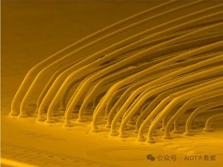
Figure 1: Wirebond wires in packages. Source: K&S
图 1:封装中的引线键合线。来源:K&S
PERFORMANCE & OPTIMIZATION COMPARISON:
性能和优化比较:
Electrical Performance: Flip Chip technology generally offers the superior electrical performance option due to its shorter interconnection lengths. This results in lower parasitic resistance, inductance, and capacitance.
电气性能:倒装芯片技术由于其较短的互连长度,通常提供卓越的电气性能选择。这会降低寄生电阻、电感和电容。
Wire Bonding, while not as efficient, can still achieve good performance for many applications, especially when using design recommendations such as:
引线键合虽然效率不高,但仍然可以在许多应用中实现良好的性能,特别是在使用以下设计建议时:
oIdentifying and optimizing critical signals
识别和优化关键信号
oPaying careful attention to die pad ring design and placement
仔细注意芯片焊盘环的设计和放置
oSelecting the most suitable wire bond diameter
选择最合适的焊线直径
oOptimizing substrate signal path connectivity
优化基板信号路径连接
Thermal Performance: Flip Chip packages typically have better thermal performance due to the direct contact between chip and substrate. However, wire bonded packages can improve upon thermal performance by implementing the following:
热性能:由于芯片和基板之间的直接接触,倒装芯片封装通常具有更好的热性能。然而,引线接合封装可以通过实施以下措施来提高热性能:
oAdding a thermal ball matrix in BGA packages
在 BGA 封装中添加热球矩阵
oIncreasing the substrate layer count
增加基材层数
oMaximizing the via count on the die attach pad
最大化芯片连接垫上的通孔数量
oBeefing up copper plane thickness
增加铜平面厚度
oEmploying heatsinks, slugs, etc.
使用散热器、散热片等。
oUtilizing filled vias 利用填充过孔
Size & Density: Flip Chip technology allows for higher I/O density and smaller package sizes. Wire Bonding requires more space due to the need for bond pads around the chip periphery and the arc of the wire bonds. However, Wire Bonding can still achieve high density in some applications through techniques like staggered bond pad arrangements.
尺寸和密度:倒装芯片技术可实现更高的 I/O 密度和更小的封装尺寸。由于需要围绕芯片外围的焊盘和引线键合的弧度,引线键合需要更多的空间。然而,在某些应用中,引线键合仍然可以通过交错键合焊盘排列等技术实现高密度。
Cost Considerations: A cost comparison between Wire Bonding and Flip Chip technology is not straight-forward. Cost comparisons can be heavily influenced by type of application, case-specific issues, and additional factors such as:
成本考虑因素:引线键合和倒装芯片技术之间的成本比较并不简单。成本比较可能会受到应用程序类型、具体案例问题以及其他因素的严重影响,例如:
oDie & wafer-level issues (e.g., bond pad pitch, configuration)
芯片和晶圆级问题(例如,焊盘间距、配置)
oDie cost & yield 模具成本和产量
oType of Flip Chip bumping technology used
使用的倒装芯片凸块技术的类型
oPackage assembly flow 封装组装流程
oProcess Total-Cost-of-Ownership (TCO)
流程总体拥有成本 (TCO)
oProduction volumes 产量
Costing Overview: Wire Bonding seems the more cost-effective method for lower I/O counts and lower production volumes. In non-leading-edge applications, Wire Bonding is considered the more cost-effective of the two IC packaging interconnect solutions. However, Flip Chip technology becomes more the more economical option when I/O count increases and for higher production volumes; mainly due to its smaller die area, that allows for more dies per wafer at a reduced cost per unit.
成本概述:对于较少的 I/O 数量和较低的产量,引线键合似乎是更具成本效益的方法。在非前沿应用中,引线键合被认为是两种IC 封装互连解决方案中更具成本效益的。然而,当 I/O 数量增加且产量更高时,倒装芯片技术就成为更经济的选择;主要是由于其芯片面积较小,因此每个晶圆可以容纳更多芯片,同时降低单位成本。
Manufacturability: When it comes to manufacturing process compatibility and ease of assembly, Wire Bonding remains the more flexible option, allowing for fewer complex design changes and faster turnaround times. Flip Chip requires more precise alignment and involves a more complex assembly process. However, in high-volume production, Flip Chip is more advantageous due to its potential for increased productivity.
可制造性:在制造工艺兼容性和组装简易性方面,引线键合仍然是更灵活的选择,可以减少复杂的设计更改并缩短周转时间。倒装芯片需要更精确的对准,并涉及更复杂的组装过程。然而,在大批量生产中,倒装芯片由于其提高生产率的潜力而更具优势。
Reliability: When properly implemented, both technologies can achieve high reliability. Wire Bonding boasts an established history of proven reliability for a wide range of applications. Flip Chip however provides outstanding reliability, particularly in harsh environments, due to shorter interconnects and underfill. Underfills are used for mechanical stabilization and protection, compensating for material stresses and reducing coefficient of thermal expansion (CTE), in electronic assemblies, especially Flip Chips.
可靠性:如果实施得当,这两种技术都可以实现高可靠性。引线键合拥有在各种应用中经过验证的可靠性的悠久历史。然而,由于更短的互连和底部填充,倒装芯片提供了出色的可靠性,特别是在恶劣的环境中。底部填充胶用于电子组件(尤其是倒装芯片)中的机械稳定性和保护、补偿材料应力并降低热膨胀系数 (CTE)。
At a Glance Comparison: 概览比较:
| Feature 特征 | Flip Chip 倒装芯片 | Wire Bond 焊线 |
| I/O Density 输入/输出密度 |
Higher I/O density, allows smaller, more compact chip packages, resulting in increased functionality. 更高的 I/O 密度可实现更小、更紧凑的芯片封装,从而增强功能。 |
Lower I/O density, requires larger chip package sizes, with lower functionality. I/O 密度较低,需要较大的芯片封装尺寸,且功能较低。 |
|
Interconnect 互连 Length 长度 |
Shorter interconnect lengths allow better electrical performance and lower ‘parasitic’ or (stray capacitance). 较短的互连长度可实现更好的电气性能和更低的“寄生”或(杂散电容)。 |
Longer, thinner interconnect lengths due to wires, result in less effective electrical performance and higher ‘parasitic’ or (stray capacitance). 由于电线而导致互连长度更长、更细,导致有效的电气性能降低和更高的“寄生”或(杂散电容)。 |
| Heat Dissipation 散热 |
Improved heat dissipation, reduces the risk of overheating. 改善散热,降低过热风险。 |
Less effective heat dissipation due to limited surface area for heat transfer. 由于传热表面积有限,散热效果较差。 |
| Package Size 包装尺寸 |
Smaller chip packages, allows for smaller electronic devices. Vertical stacking and 3D IC integration are easily achieved. 更小的芯片封装允许更小的电子设备。可以轻松实现垂直堆叠和 3D IC 集成。 |
Wires between chip and bond pad can be longer, resulting in a larger footprint. Vertical stacking is far more complex. 芯片和焊盘之间的电线可以更长,从而导致更大的占地面积。垂直堆叠要复杂得多。 |
| Design 设计 |
More design complexity due to higher interconnection density. Requires precise alignment of pitch pads and solder bumps. 由于互连密度更高,设计变得更加复杂。需要精确对准间距焊盘和焊料凸块。 |
Simpler design due to fewer I/O connections and less precision needed to attach wires to the bond pads. 由于 I/O 连接较少,并且将导线连接到焊盘所需的精度较低,因此设计更加简单。 |
| Costing 成本核算 |
At high volume and high manufacturing yields flip-chip can be more cost effective. The smaller die area fits more dies per wafer, reducing cost per unit. 在大批量和高制造产量的情况下,倒装芯片可以更具成本效益。较小的芯片面积可以在每个晶圆上容纳更多的芯片,从而降低单位成本。 |
For non-leading-edge applications Wire Bonding is the most likely cost-effective packaging solution. 对于非前沿应用,引线键合是最有可能具有成本效益的封装解决方案。 |
| Process Nodes 流程节点 |
Can be used for advanced process nodes in the rage of 7nm / 5nm. 可用于7nm/5nm时代的先进工艺节点。 |
Can be used for more mature process nodes, in the rage 28nm / 14nm. 可用于更成熟的工艺节点,流行的有28nm/14nm。 |
USE-CASES & APPLICATIONS 用例和应用
Common Wire Bonding Applications: This basic technique is widely used in microelectronic products for a wide range of industries and applications, mainly because of its cost-efficiency, versatility and reliability:
常见引线键合应用:这种基本技术广泛应用于各种行业和应用的微电子产品,主要是因为其成本效益、多功能性和可靠性:
oIntegrated Circuits (ICs): Wire Bonding is still the dominant technology used in connecting IC chips to packages, especially for mature process nodes (28nm and above).
集成威廉希尔官方网站
(IC) :引线键合仍然是连接 IC 芯片与封装的主要技术,特别是对于成熟的工艺节点(28 纳米及以上)。
oSensors: Many sensory devices, such as pressure sensors, temperature sensors, and accelerometers, use Wire Bonding for electrical connections.
传感器:许多传感设备,例如压力传感器、温度传感器和加速度计,都使用引线键合进行电气连接。
oOptoelectronics: Devices like LEDs, photodiodes, and laser diodes regularly use Wire Bonding for electrical and optical signal transmission connections.
光电器件:LED、光电二极管和激光二极管等器件经常使用引线键合进行电信号和光信号传输连接。
oPower Devices: MOSFETs and insulated gate bipolar transistors (IGBTs) frequently use Wire Bonding for power connections.
功率器件:MOSFET 和绝缘栅双极晶体管 (IGBT) 经常使用引线键合进行电源连接。
oMemory Devices: Many memory chips, especially those not requiring super high performance, use Wire Bonding.
存储器件:许多存储芯片,尤其是那些不需要超高性能的存储芯片,都使用引线键合。
Common Flip Chip Applications: In answer to market demand for quality high-speed and high-performance package design, the most commonly used packaging solution for these more advanced applications is flip chip technology:
常见的倒装芯片应用:为了满足市场对高质量高速和高性能封装设计的需求,这些更先进的应用最常用的封装解决方案是倒装芯片技术:
oHigh-Performance Processors: CPUs and GPUs for computers and servers require Flip Chip technology to achieve the highest performance and I/O density.
高性能处理器:计算机和服务器的 CPU 和 GPU 需要倒装芯片技术来实现最高的性能和 I/O 密度。
oAdvanced Mobile Devices: Smartphones and tablets increasingly use Flip Chip technology in their main processors and other high-performance components.
先进移动设备:智能手机和平板电脑越来越多地在其主处理器和其他高性能组件中使用倒装芯片技术。
oNetworking Equipment: High-speed routers and switches need the kind of improved electrical performance Flip Chip packaging can deliver.
网络设备:高速路由器和交换机需要倒装芯片封装能够提供的改进电气性能。
oAutomotive Electronics: Advanced driver assistance systems (ADAS) and other high-performance automotive electronics are readily adopting Flip Chip technology. See also: Automotive PCBs
汽车电子:先进驾驶辅助系统(ADAS)和其他高性能汽车电子很容易采用倒装芯片技术。另请参阅:汽车 PCB
oHigh-Frequency RF Devices: The shorter interconnects in Flip Chip technology make it an ideal solution for high-frequency applications in wireless communications.
高频射频器件:倒装芯片技术中较短的互连使其成为无线通信中高频应用的理想解决方案。
EYE ON THE FUTURE 着眼未来
Monitoring Future Trends: Both Wire Bonding and Flip Chip continue to evolve, with a view towards meet pressing market demand for vastly improved near-future electronic device technology.
监控未来趋势:引线键合和倒装芯片都在不断发展,以满足市场对近期电子设备技术大幅改进的迫切需求。
| Wire Bonding Trends 引线键合趋势 | Flip Chip Trends 倒装芯片趋势 |
|
Development of finer pitch bonding capabilities 开发更细间距的接合能力 Alternative wire materials (e.g., copper) for improved performance and costing 替代电线材料(例如铜)可提高性能和成本 Advancements in equipment and process control for higher efficiency and reliability 设备和过程控制的进步提高了效率和可靠性 |
Continued miniaturization of solder bumps for even higher I/O densities 焊料凸点持续小型化,以实现更高的 I/O 密度 Development of advanced underfill materials for improved reliability 开发先进的底部填充材料以提高可靠性 Integration with other advanced packaging technologies, such as 2.5D and 3D 与其他先进封装技术集成,例如 2.5D 和 3D |
Final Thoughts: The choice between Wire Bonding and Flip Chip depends on various factors, including electrical and thermal requirements, size constraints, production volume, and cost considerations. As the electronics industry continues to demand higher performance and smaller form factors, both technologies will likely coexist, with each finding its niche in different applications and market segments.
最后的想法:引线键合和倒装芯片之间的选择取决于多种因素,包括电气和热要求、尺寸限制、产量和成本考虑。随着电子行业不断要求更高的性能和更小的外形尺寸,这两种技术可能会共存,每种技术都会在不同的应用和细分市场中找到自己的定位。
As the benefits of Moore’s law reach their limits, advances in chip performance rely more on the back end of production, including packaging.
随着摩尔定律的优势达到极限,芯片性能的进步更多地依赖于包括封装在内的生产后端
Semiconductor wafers are the basis of the integrated circuits so crucial to most of today’s technology. The wafers’ packaging—whether metal, plastic, ceramic, or glass—connects them to their environment and protects them from chemical contamination and damage from light, heat, and impacts. Compared with the front-end process of designing and fabricating wafers, the back-end process of packaging has been undervalued for two reasons: First, it’s still possible to package wafers using old-generation equipment. Second, packaging is mostly done by outsourced semiconductor assembly and test companies (OSATs) that compete largely based on low labor costs, rather than other sources of differentiation.
半导体晶圆是集成威廉希尔官方网站 的基础,对当今大多数技术至关重要。晶圆的包装(无论是金属、塑料、陶瓷还是玻璃)将它们与环境连接起来,并保护它们免受化学污染以及光、热和冲击造成的损坏。与设计和制造晶圆的前端工艺相比,封装的后端工艺被低估,原因有二:首先,仍然可以使用老一代设备来封装晶圆。其次,封装主要由外包半导体组装和测试公司(OSAT)完成,这些公司主要基于低劳动力成本而不是其他差异化来源进行竞争。
This model may change with the introduction of advanced packaging, which uses sophisticated technology and aggregates components from various wafers, creating a single electronic device with superior performance. Introduced around 2000, advanced packaging is now gaining significant momentum as the next breakthrough in semiconductor technology.
这种模式可能会随着先进封装的引入而改变,先进封装使用复杂的技术并聚合来自各种晶圆的组件,创造出具有卓越性能的单一电子设备。先进封装于 2000 年左右推出,目前作为半导体技术的下一个突破正在获得巨大的发展势头。
Advanced packaging is helping to meet the demand for semiconductors that run emerging applications now going mainstream—for example, 5G, autonomous vehicles and other Internet of Things technologies, and virtual and augmented reality. These applications require high-performance, low-power chips that can rapidly process massive quantities of data. Despite Moore’s law, which in 1965 posited that the number of transistors on a microchip would double every couple of years, node advancement is now reaching its limits. As a result, technical advances on the front end of chip manufacturing are slowing, and the economically viable maximum size of a die, and thus its performance, are becoming more limited. New approaches in back-end technology that combine multiple chips offer a promising solution. Advanced-packaging techniques that have arisen over the past two decades—including 2.5-D, 3-D, fan-out, and system-on-a-chip (SoC) packaging—promise to fill the void by supplementing the wire-bonding and flip-chip technologies of the previous half century.
先进封装有助于满足对运行现已成为主流的新兴应用(例如 5G、自动驾驶汽车和其他物联网技术以及虚拟和增强现实)的半导体的需求。这些应用需要高性能、低功耗的芯片,能够快速处理大量数据。尽管摩尔定律在 1965 年规定微芯片上的晶体管数量每隔几年就会翻一番,但节点的进步现在已经达到了极限。因此,芯片制造前端的技术进步正在放缓,经济上可行的芯片最大尺寸及其性能也变得更加有限。结合多个芯片的后端技术新方法提供了一个有前途的解决方案。过去二十年出现的先进封装技术(包括 2.5D、3D、扇出和片上系统 (SoC) 封装)有望通过补充引线键合来填补空白以及前半个世纪的倒装芯片技术。
Because advanced packaging offers a higher-value opportunity than traditional back-end packaging, major players and fast followers (organizations that imitate competitors’ innovations) are developing and commercializing various forms of the technology to win premium customers. In this article, we describe how the market is evolving and suggest how manufacturers can take advantage of the opportunities becoming available.
由于先进封装提供了比传统后端封装更高价值的机会,因此主要参与者和快速追随者(模仿竞争对手创新的组织)正在开发各种形式的技术并将其商业化,以赢得优质客户。
Key advanced-packaging technologies
先进封装关键技术
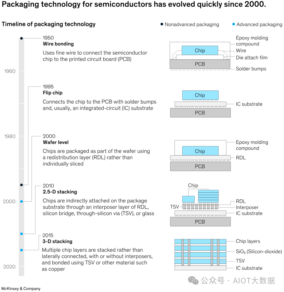
Three major advanced-packaging technologies have become commercially available since 2000, supplementing the two technologies that prevailed during the previous half century (Exhibit 1).
自 2000 年以来,三种主要的先进封装技术已投入商业应用,补充了过去半个世纪盛行的两种技术(图表 1)。
Traditional packaging techniques
传统包装技术
Developed in the 1950s and still in use today, wire-bond technology is an interconnection technique that attaches the printed circuit board (PCB) to the die—the silicon square that contains the integrated circuit—using solder balls and thin metal wires. It requires less space than packaged chips and can connect relatively distant points, but it can fail in high temperatures, high humidity, and temperature cycling, and each bond must be formed sequentially, which adds complexity and can slow manufacturing. The wire-bonding market is expected to be valued at about $16 billion by 2031, with a CAGR of 2.9 percent.
引线键合技术开发于 20 世纪 50 年代,至今仍在使用,它是一种互连技术,使用焊球和细金属线将印刷威廉希尔官方网站
板 (PCB) 连接到芯片(包含集成威廉希尔官方网站
的硅方块)。它比封装芯片需要更少的空间,并且可以连接相对较远的点,但它可能会在高温、高湿度和温度循环中失效,并且每个键必须顺序形成,这增加了复杂性并会减慢制造速度。预计到 2031 年,引线键合市场价值将达到约 160 亿美元,复合年增长率为 2.9%。
The first major evolution in packaging technology came in the mid-1990s with flip chips, which use a face-down die, the entire surface area of which is used for interconnection through solder “bumps” that bond the PCB with the die. This results in a smaller form factor, or hardware size, and a higher signal-propagation rate—that is, faster movement of signals from the transmitter to the receiver. Flip-chip packaging is the most common and lowest-cost technology currently in use, mainly for central processing units, smartphones, and radio-frequency system-in-package solutions. Flip chips allow for smaller assembly and can handle higher temperatures, but they must be mounted on very flat surfaces and are not easy to replace. The current flip-chip market is around $27 billion, with a projected CAGR of 6.3 percent, which should bring it to $45 billion by 2030.
封装技术的第一次重大发展出现在 20 世纪 90 年代中期的倒装芯片中,它使用面朝下的芯片,其整个表面区域用于通过将 PCB 与芯片粘合的焊料“凸块”进行互连。这导致更小的外形尺寸或硬件尺寸以及更高的信号传播速率,即信号从发射器到接收器的更快移动。倒装芯片封装是目前使用最常见、成本最低的技术,主要用于中央处理器、智能手机和射频系统级封装解决方案。倒装芯片允许更小的组装并且可以承受更高的温度,但它们必须安装在非常平坦的表面上并且不容易更换。当前倒装芯片市场规模约为 270 亿美元,预计复合年增长率为 6.3%,到 2030 年将达到 450 亿美元.
Wafer-level packaging 晶圆级封装
While traditional packaging “dices” the silicon wafer into individual chips first and then attaches the chips to the PCB and builds the electrical connections, wafer-level packaging makes the electrical connections and molding at the wafer level, then dices the chips using a laser. The greatest difference between wafer-level chip-scale packaging (WLCSP) and flip chips in terms of chip configuration is that WLCSPs have no substrate between the die and the PCB. Instead, redistribution layers (RDLs) replace the substrate, leading to a smaller package and enhanced thermal conduction.
传统封装首先将硅晶圆“切割”成单独的芯片,然后将芯片附着到 PCB 上并建立电气连接,而晶圆级封装则在晶圆级进行电气连接和成型,然后使用激光切割芯片。晶圆级芯片级封装 (WLCSP) 和倒装芯片在芯片配置方面的最大区别在于,WLCSP 的芯片和 PCB 之间没有基板。相反,重新分布层 (RDL) 取代了基板,从而缩小了封装并增强了导热性。
Wafer-level packaging is divided into two types: fan-in and fan-out. In fan-in wafer-level packaging, used mainly for low-end mobile phones that require rudimentary technology, the RDLs are routed toward the center of the die. In the fan-out version, which was introduced in 2007, the RDL and solder balls exceed the size of the die, so the chip can have more inputs and outputs while maintaining a thin profile.3 Fan-out packaging comes in three types: core, high density, and ultrahigh density. Core, which is used mostly for automotive and network applications that don’t require high-end technology—such as radio frequency and infotainment chips—accounts for less than 20 percent of the almost $1.5 billion fan-out packaging market. High and ultrahigh density are mostly used for mobile applications and are expected to expand to some network and high-performance computing applications. The world’s largest maker of WLCSPs is the Taiwan Semiconductor Manufacturing Company (TSMC).
晶圆级封装分为扇入型和扇出型两种。在主要用于需要基本技术的低端手机的扇入式晶圆级封装中,RDL 被布线到芯片的中心。在 2007 年推出的扇出版本中,RDL 和焊球超出了芯片的尺寸,因此芯片可以拥有更多的输入和输出,同时保持薄型。 3扇出封装分为三种类型:核心封装、高密度封装和超高密度封装。核心主要用于不需要高端技术(例如射频和信息娱乐芯片)的汽车和网络应用,在近 15 亿美元的扇出封装市场中所占比例不到 20%。高密度和超高密度主要用于移动应用,预计将扩展到一些网络和高性能计算应用。全球最大的 WLCSP 制造商是台湾积体威廉希尔官方网站
制造公司 (TSMC)。
The past decade saw the development of stacked WLCSP, which allows for multiple integrated circuits in the same package and is used for both heterogeneous bonding, which integrates logic and memory chips, and memory-chip stacking. In 2.5-D stacking, two or more chips are laid side by side with an interposer connecting one die to another. There are several categories of 2.5-D stacking, based on the kind of interposer it uses:
过去十年见证了堆叠式 WLCSP 的发展,它允许在同一封装中集成多个集成威廉希尔官方网站
,并可用于集成逻辑和存储芯片的异构键合以及存储芯片堆叠。在 2.5 维堆叠中,两个或多个芯片并排放置,并通过中介层将一个芯片连接到另一个芯片。根据所使用的中介层类型,2.5 维堆叠可分为多种类别:
·Silicon interposers are the only type that requires TSV, or through-silicon via—a vertical electrical connection that passes through the silicon die or wafer. Silicon interposers use a stable technology that has been on the market for more than ten years, but the cost of silicon is high and requires front-end technology and manufacturing capability. TSMC’s CoWoS-S (chip on wafer on substrate) dominates the market.
硅中介层是唯一需要 TSV 或硅通孔(一种穿过硅芯片或晶圆的垂直电气连接)的类型。硅中介层采用的是已经上市十多年的稳定技术,但硅的成本较高,并且需要前端技术和制造能力。台积电的CoWoS-S(基板上晶圆芯片)占据市场主导地位。
·Silicon bridges are relatively new. Because they use smaller amounts of silicon than traditional silicon interposers, they are thinner, which reduces power consumption and increases design flexibility. Their advantage over traditional silicon interposers is that they can enable more advanced system-level integration, so they are used for high-performance computing (HPC) such as AI. Representative technologies include Intel’s EMIB (embedded multi-die interconnect bridge) and TSMC’s CoWoS-L.
硅桥相对较新。由于它们比传统硅中介层使用更少的硅,因此更薄,从而降低了功耗并提高了设计灵活性。与传统硅中介层相比,它们的优势在于可以实现更先进的系统级集成,因此它们用于人工智能等高性能计算(HPC)。代表性技术包括英特尔的EMIB(嵌入式多芯片互连桥)和台积电的CoWoS-L。
·Redistribution layers can also function as interposers. The greatest strength of this technology is that the photolithography process that creates RDLs allows for fine patterning, which improves speed gain and heat dissipation. TSMC’s CoWoS-R (chip-on-wafer-on-substrate RDL) is set to begin mass-volume production.
重新分布层也可以充当中介层。该技术的最大优势在于,创建 RDL 的光刻工艺可实现精细图案化,从而提高速度增益和散热。台积电的 CoWoS-R(晶圆上芯片 RDL)即将开始量产。
·Glass is also rising as a next-generation material for interposers. It offers low cost and low power loss in high-frequency bandwidths, but it may not be marketable for some time.
玻璃也正在成为下一代中介层材料。它在高频带宽中提供低成本和低功耗,但可能在一段时间内无法上市。
In 3-D stacking, multiple chips are placed face down on top of one another, with or without an interposer. There are two main types of 3-D stacking. The most common type is TSV with micro-bumps (µ-bumps). The newer alternative, bumpless hybrid bonding, forms interconnections using a dielectric bond and embedded metal; it is just being explored by memory players.
在 3D 堆叠中,多个芯片面朝下堆叠在一起,无论有或没有中介层。3D 堆叠有两种主要类型。最常见的类型是带有微凸块(μ 凸块)的 TSV。较新的替代方案是无凸点混合键合,使用电介质键合和嵌入式金属形成互连;它只是被记忆玩家探索而已。
How will the market evolve?
市场将如何发展?
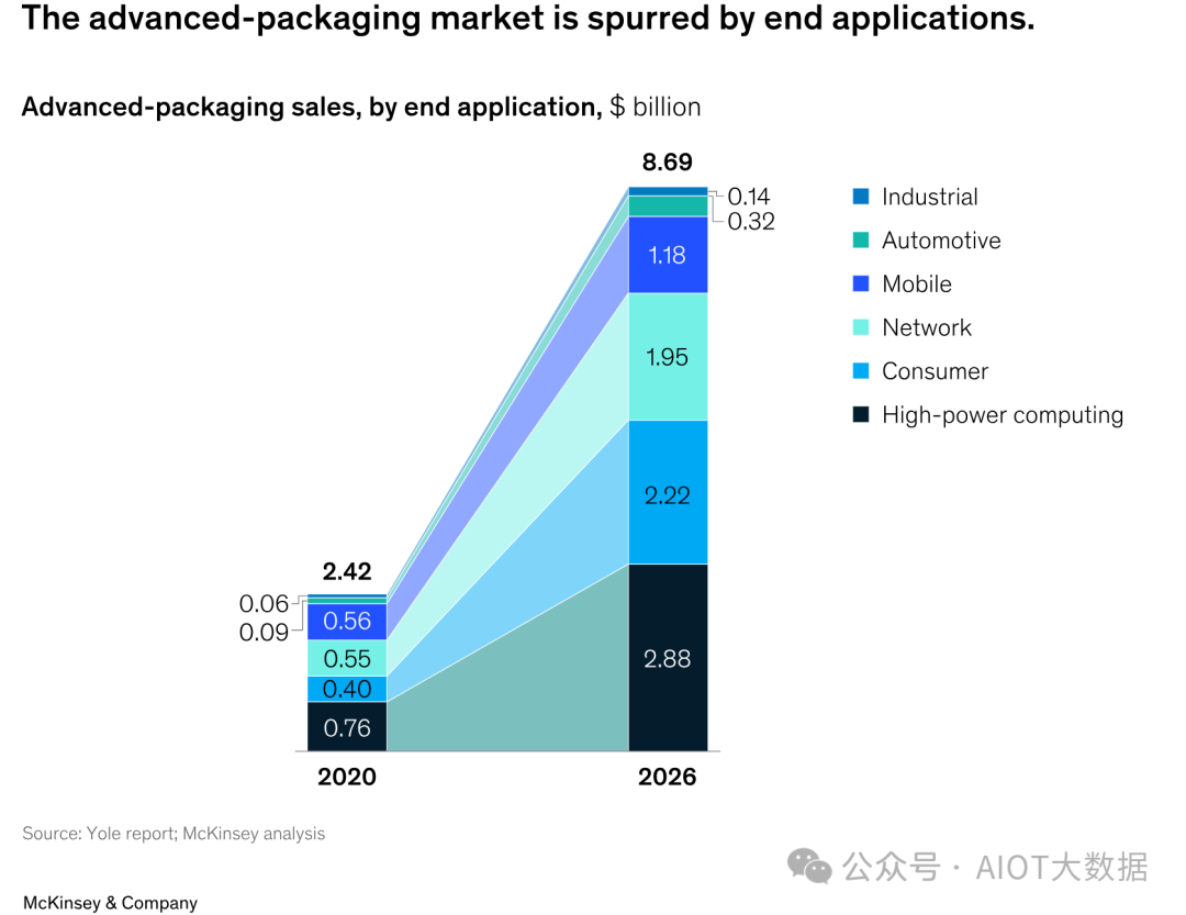
The advanced-packaging market is driven by the end applications of its various technologies (Exhibit 2). Since the mid-2010s, fan-out wafer-level packaging has dominated, with about 60 percent market share. Fan-out packaging is cheaper than stacking and is engineered for high heat resistance and a small form factor. These attributes make it appropriate for mobile applications, which are likely to generate most of its demand.
先进封装市场由各种技术的最终应用驱动(图表 2)。自 2010 年代中期以来,扇出晶圆级封装占据主导地位,占据约 60% 的市场份额。扇出封装比堆叠封装更便宜,并且专为高耐热性和小外形而设计。这些属性使其适合移动应用程序,而移动应用程序可能会产生大部分需求。
Apple uses fan-out advanced packaging for its application processors, graphic chips, and 5G and 6G modem chips. It is the largest user of the technology, consuming most of the volume produced by TSMC. Other top fabless players—that is, companies that design and sell hardware and chips but outsource their manufacture—are also using fan-out technology in mass-produced chips.
苹果公司的应用处理器、图形芯片以及 5G 和 6G 调制解调器芯片采用扇出先进封装。它是该技术的最大用户,消耗了台积电生产的大部分产量。其他顶级无晶圆厂厂商——即设计和销售硬件和芯片但外包制造的公司——也在批量生产的芯片中使用扇出技术。
Most of the growth in HPC and network applications is likely to come from AI chips, edge computing, and network chips in consumer devices, which require the small form factor and affordable cost that fan-out packaging can offer.
HPC 和网络应用的大部分增长可能来自消费设备中的人工智能芯片、边缘计算和网络芯片,这些芯片需要扇出封装能够提供的小外形尺寸和可承受的成本。
The most likely driver of growth in 2.5-D stacking could be HPC applications, which are in high demand for data centers. Although less than 20 percent of data-center capacity used 2.5-D stacking in 2022, the rate could increase to 50 percent in the next five years. For mobile applications, 2.5-D packaging is considered too costly, but this may change with the arrival of the next generation, which will feature less expensive silicon bridges, RDLs, and glass interposers.
2.5 维堆叠增长最有可能的推动力可能是 HPC 应用程序,数据中心对 HPC 应用程序的需求很高。尽管到 2022 年,只有不到 20% 的数据中心容量使用 2.5 维堆叠,但这一比例在未来五年内可能会增加到 50%。对于移动应用,2.5D 封装被认为成本太高,但随着下一代的到来,这种情况可能会改变,下一代封装将采用更便宜的硅桥、RDL 和玻璃中介层。
For 3-D packaging, memory—the dominant application for 3-D stacking—and SoC use are expected to grow at a CAGR of roughly 30 percent. Increasingly, 3-D stacked memory is being incorporated with logic chips for high-performance products that require high bandwidth, including high-bandwidth memory (HBM) and processing in memory with HBM (PIM-HBM). Substantial demand for 3-D stacked memory will likely come from data-center servers, which require high capacity and high speed, and graphics accelerators and network devices, which require the maximum possible bandwidth for memory and processing.
对于 3D 封装、内存(3D 堆叠的主要应用)和 SoC 的使用预计将以大约 30% 的复合年增长率增长。3D 堆叠存储器越来越多地与需要高带宽的高性能产品的逻辑芯片相结合,包括高带宽存储器 (HBM) 和采用 HBM 的存储器处理 (PIM-HBM)。对 3D 堆栈内存的大量需求可能来自需要高容量和高速度的数据中心服务器,以及需要尽可能大的内存和处理带宽的图形加速器和网络设备。
HPC systems, specifically CPUs, will drive demand for 3-D SoC chips. Major players started adopting hybrid bonding in 2022, and fast followers may join the market soon. OSATs, lower-tier foundries, and integrated device manufacturers (IDMs) are unlikely to enter the market, given the high technology barrier.
HPC 系统,特别是 CPU,将推动对 3D SoC 芯片的需求。主要参与者于 2022 年开始采用混合粘合,快速追随者可能很快就会加入市场。鉴于技术壁垒较高,OSAT、低端代工厂和集成设备制造商 (IDM) 不太可能进入该市场。
Key market-winning capabilities
赢得市场的关键能力
Market growth relies heavily on end customers, such as automotive OEMs and home appliance manufacturers. More end customers are seeking advanced-packaging providers because of the growing need for fast, reliable computing for applications such as autonomous vehicles. For semiconductor manufacturers—especially logic IDMs and foundries—advanced packaging could be a key selling point.
市场增长很大程度上依赖于最终客户,例如汽车原始设备制造商和家电制造商。由于自动驾驶汽车等应用对快速、可靠计算的需求不断增长,越来越多的最终客户正在寻求先进的封装提供商。对于半导体制造商(尤其是逻辑 IDM 和代工厂)而言,先进封装可能是一个关键卖点。
More end customers are seeking advanced-packaging providers because of the growing need for fast, reliable computing for applications such as autonomous vehicles.
由于自动驾驶汽车等应用对快速、可靠计算的需求不断增长,越来越多的最终客户正在寻求先进的封装提供商。
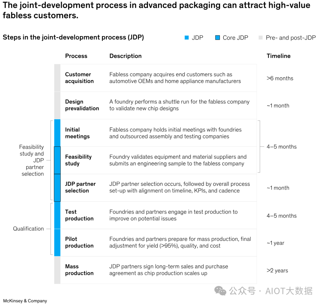
To acquire and retain high-value fabless customers, manufacturers need to be comfortable codeveloping advanced-packaging solutions. While fabless players take full ownership of the chip-planning process before at-scale production begins, there is room for manufacturers to add value. Joint development often occurs during the chip-architecture design stage and initial shuttle runs for design validation (Exhibit 3). The need for such cooperation is expected to increase because of the demand for higher-performance chips and the increased complexity of chip designs created by packaging.
为了获得并留住高价值的无晶圆厂客户,制造商需要轻松地共同开发先进封装解决方案。尽管无晶圆厂厂商在大规模生产开始之前完全掌控了芯片规划流程,但制造商仍有增加价值的空间。联合开发通常发生在芯片架构设计阶段和用于设计验证的初始穿梭运行期间(图表 3)。由于对更高性能芯片的需求以及封装带来的芯片设计复杂性的增加,预计这种合作的需求将会增加。
In 2016, TSMC released innovative integrated fan-out (InFO) wafer-level systems, mainly for wireless applications, in close collaboration with its lead customer. More recently, derivatives of that, such as InFO AiP (antenna in package) and InFO PoP (package on package), have been released to expand into other applications for networking and HPC.
2016年,台积电与其主要客户密切合作,发布了创新的集成扇出(InFO)晶圆级系统,主要用于无线应用。最近,InFO AiP(封装内天线)和 InFO PoP(封装上封装)等衍生产品已发布,可扩展到网络和 HPC 的其他应用。
Fast followers may have a hard time catching up with market leaders, because huge technology investments would be required to assure customers of the volume to support products. In addition, although fast followers may have R&D-level packaging technology for fan-out and 2.5-D, they have little or no production experience, which is essential for high production yield. To overcome this, packaging players would need to acquire anchor customers from the initial stages of development. Positioning their companies as willing to help manufacture products for advanced packaging from the design stage would be key to acquiring customers.
快速追随者可能很难赶上市场领导者,因为需要巨额技术投资才能向客户保证支持产品的数量。此外,尽管快速追随者可能拥有扇出和2.5D的研发级封装技术,但他们几乎没有或根本没有生产经验,而这对于高生产良率至关重要。为了克服这个问题,包装企业需要从发展的初始阶段就获得固定客户。将他们的公司定位为愿意从设计阶段帮助制造先进封装产品将是获取客户的关键。
Advanced packaging requires changes in the architecture of end-user software and hardware, so packaging design should be considered during the initial architecture stage, when support from back-end providers can lower the burden of adopting advanced packaging. Once a customer selects an advanced-packaging vendor, it will likely commit to that vendor for future projects as well.
先进封装需要改变最终用户软件和硬件的架构,因此应在初始架构阶段考虑封装设计,此时后端提供商的支持可以减轻采用先进封装的负担。一旦客户选择了先进封装供应商,他们很可能也会在未来的项目中选择该供应商。
To acquire design capabilities, companies can partner with or invest in a design house. Design houses play a critical role across the entire chip-making process, from intellectual-property (IP) development to design and production. Additionally, owning an IP pool can help customers meet their design needs quickly and allow them to avoid redundant designs and resources. Design houses should be able to offer front- and back-end services. Front-end services include register-transfer-level design and high-level description of the functions required; back-end design includes logic testing and place and route.
为了获得设计能力,公司可以与设计公司合作或投资设计公司。设计公司在从知识产权 (IP) 开发到设计和生产的整个芯片制造过程中发挥着关键作用。此外,拥有IP池可以帮助客户快速满足他们的设计需求,并让他们避免冗余的设计和资源。设计公司应该能够提供前端和后端服务。前端服务包括寄存器传输级设计和所需功能的高层描述;后端设计包括逻辑测试和布局布线。
Another potentially important value proposition for the chip manufacturer is securing design capabilities and providing turnkey solutions—from design to wafer manufacturing, packaging, and testing. This type of offering provides customers with a one-stop shop.
对于芯片制造商来说,另一个潜在的重要价值主张是确保设计能力并提供从设计到晶圆制造、封装和测试的交钥匙解决方案。此类产品为客户提供一站式服务。
In terms of manufacturing, the two key technological capabilities manufacturers need to master for 2.5-D and 3-D packaging are, respectively, interposers and hybrid bonding. For 2.5-D, manufacturers must be able to handle emerging interposer solutions using novel materials and manufacturing methodologies, including silicon, RDL, and glass. For 3-D, the latest technology, hybrid bonding, requires chemical mechanical planarization to polish various substances with equal flatness and prevent dishing, as well as high interconnect accuracy through disk-to-wafer capabilities in both equipment and know-how.
在制造方面,2.5D和3D封装制造商需要掌握的两项关键技术能力分别是中介层和混合键合。对于 2.5D,制造商必须能够使用新型材料和制造方法(包括硅、RDL 和玻璃)来处理新兴中介层解决方案。对于 3D 技术,混合键合需要化学机械平坦化,以相同的平坦度抛光各种物质并防止凹陷,以及通过设备和技术中的磁盘到晶圆功能实现高互连精度。
Implications for manufacturers
对制造商的影响
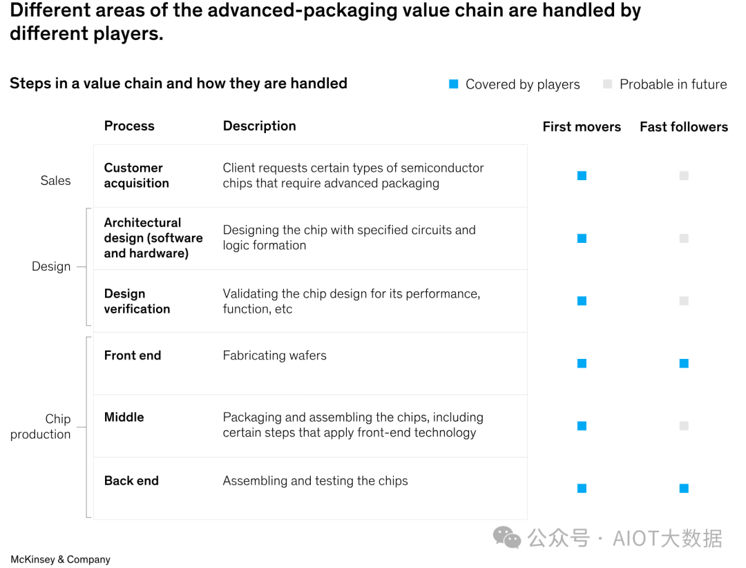
Key players in advanced packaging include logic and memory IDMs, foundries with leading or mature node capabilities, and OSATs. Exhibit 4 shows the capabilities currently handled by first movers and fast followers.
先进封装的主要参与者包括逻辑和存储器 IDM、具有领先或成熟节点能力的代工厂以及 OSAT。图表 4 显示了先行者和快速追随者当前所具备的能力。
First movers 先行者
First movers have entered the market and are in mass-volume production based on their logic-packaging capabilities. They are actively developing use cases with existing customers and applying cutting-edge advanced-packaging technologies. While these major players are advanced in R&D and manufacturing, they may seek partnerships with followers to stabilize volume as they face rapidly expanding demand.
先行者已经进入市场,并基于其逻辑封装能力进行批量生产。他们正在积极与现有客户一起开发用例并应用尖端的先进封装技术。虽然这些主要参与者在研发和制造方面处于领先地位,但在面临快速增长的需求时,他们可能会寻求与追随者合作以稳定产量。
First movers are in mass-volume production based on their logic-packaging capabilities. While these players are advanced in R&D and manufacturing, they may seek partnerships with followers to stabilize volume as they face rapidly expanding demand.
先行者凭借其逻辑封装能力实现了大批量生产。尽管这些企业在研发和制造方面处于领先地位,但在面临快速增长的需求时,他们可能会寻求与追随者的合作伙伴关系来稳定产量。
Fast followers 快速追随者
Many fast followers are striving to take a share of the advanced-packaging market but have not mastered the design or manufacturing capabilities or built a sufficient customer base, especially for high-end solutions.
许多快速追随者正在努力抢占先进封装市场的份额,但尚未掌握设计或制造能力,也没有建立足够的客户群,尤其是高端解决方案。
Foundries that have mature node capability but lack advanced packaging could benefit substantially from finding synergies within their current product portfolios. While advanced logic chips with nodes smaller than ten nanometers have the greatest need for advanced packaging, it is critical for fast followers to find opportunities to capture the mature-node market. Some of the areas where advanced packaging can be adapted to enhance the performance of mature-node legacy chips are radio-frequency transceiver chips for network applications, advanced driver-assist systems (ADAS), and infotainment chips for automotive applications.
拥有成熟节点能力但缺乏先进封装的代工厂可以从当前产品组合中寻找协同效应中获益匪浅。虽然节点小于十纳米的先进逻辑芯片对先进封装的需求最大,但对于快速追随者来说,寻找机会占领成熟节点市场至关重要。可以采用先进封装来增强成熟节点传统芯片性能的一些领域包括用于网络应用的射频收发器芯片、高级驾驶员辅助系统 (ADAS) 以及用于汽车应用的信息娱乐芯片。
Another option is to partner with logic providers to develop design and manufacturing solutions for specific applications that use both mature and leading-edge nodes. The feasibility of this tactic would largely depend on the end-application demand and logic providers’ needs.
另一种选择是与逻辑提供商合作,为使用成熟和领先节点的特定应用开发设计和制造解决方案。这种策略的可行性在很大程度上取决于最终应用程序的需求和逻辑提供商的需求。
OSATs OSAT
OSATs’ capabilities in the high-end advanced-packaging market are limited. Rather than trying to compete directly with high-end solutions, they can offer comparatively low-end solutions or seek to collaborate in certain value-chain areas with players capable of high-end advanced packaging. Leading OSATs are actively investing to expand the range of advanced packaging they offer. Some can already handle core and HD-level fan-out packaging, but 2.5-D and 3-D stacking mainly remain in R&D.
OSAT 在高端先进封装市场的能力有限。他们可以提供相对低端的解决方案,或者寻求在某些价值链领域与具有高端先进封装能力的厂商合作,而不是试图与高端解决方案直接竞争。领先的 OSAT 正在积极投资以扩大其提供的先进封装的范围。有些已经可以处理核心和高清级扇出封装,但 2.5 维和 3 维堆叠主要仍处于研发阶段。
Another option for OSATs is to partner with players capable of 2.5-D and 3-D stacking. While these partners work on core processes—including through-silicon via, RDL lithography, and hybrid bonding—the OSATs could offer solutions for the mid- to back-end processes, including wafer thinning and bumping.
OSAT 的另一个选择是与能够进行 2.5-D 和 3-D 堆叠的厂商合作。虽然这些合作伙伴致力于核心工艺(包括硅通孔、RDL 光刻和混合键合),但 OSAT 可以为中后端工艺(包括晶圆减薄和凸点)提供解决方案。
Although foundries and IDMs are developing advanced-packaging capabilities, they will likely use advanced packaging only to attract high-end customers that require state-of-the-art technology and, therefore, will not disrupt the entire OSAT business. They are not expected to expand into core and fan-out advanced packaging, given the significant differences in operating margin compared with front-end manufacturing, though they may make the leap into more profitable advanced 2.5-D or 3-D packaging.
尽管代工厂和 IDM 正在开发先进封装能力,但他们可能只会使用先进封装来吸引需要最先进技术的高端客户,因此不会扰乱整个 OSAT 业务。鉴于运营利润率与前端制造相比存在显着差异,预计它们不会扩展到核心和扇出先进封装领域,尽管它们可能会进军利润更高的先进 2.5-D 或 3-D 封装领域。
Memory IDMs 内存 IDM
Logic capability is essential for advanced packaging, but 3-D stacking technology can still present opportunities for memory IDMs, as top players are using it to enhance performance in memory chips that include basic-level logic chips. IDM players can also differentiate themselves by using the technology to customize memory for key clients’ advanced-packaging chips.
逻辑能力对于先进封装至关重要,但 3D 堆叠技术仍然可以为内存 IDM 提供机会,因为顶级厂商正在使用它来增强包括基础级逻辑芯片在内的内存芯片的性能。IDM厂商还可以利用该技术为主要客户的先进封装芯片定制存储器,从而使自己脱颖而出。
Another scenario for memory IDMs is to develop logic capabilities, particularly in design or manufacturing, to enable synergies with advanced packaging. This would, however, require substantial investment and a risky leap across the value chain.
内存 IDM 的另一个场景是开发逻辑功能,特别是在设计或制造方面,以实现与先进封装的协同作用。然而,这需要大量投资和跨越价值链的冒险跨越。
The advent of advanced packaging has changed the competitive landscape for chip manufacturers. Packaging is no longer a commodity process, and the majors have moved first to make advanced packaging a strategic part of their offerings. Other manufacturers risk being commoditized if they don’t find a way to incorporate advanced packaging into their strategies and offerings. The advanced-packaging market offers many disruptive opportunities, as well as challenges that will likely go beyond business as usual.
先进封装的出现改变了芯片制造商的竞争格局。包装不再是一种商品流程,各大公司已首先采取行动,将先进包装作为其产品的战略部分。其他制造商如果找不到将先进封装纳入其战略和产品的方法,则面临被商品化的风险。先进封装市场提供了许多颠覆性的机遇,也带来了可能超出常规业务的挑战。
About the author(s) 关于作者
Ondrej Burkacky is a senior partner in McKinsey’s Munich office, and Taeyoung Kim is a consultant in the Seoul office, where Inji Yeom is an associate partner.
Ondrej Burkacky是麦肯锡慕尼黑办事处的高级合伙人, Taeyoung Kim是首尔办事处的顾问, Inji Yeom是麦肯锡办事处的副合伙人。
在越南投资半导体封装的机遇与挑战
越南在半导体产业尤其是封装和测试(封测)领域正逐渐成为一个重要的投资目的地。
政府战略与目标: 越南政府已经制定了一个三阶段的半导体产业路线图,目标是在2030年之前拥有1家芯片制造厂和10家封测厂。这一战略反映了越南希望成为全球半导体产业中心之一的雄心。路线图特别强调了“C=SET+1”的策略,这里“C”代表芯片,“S”代表专用半导体,“E”代表电子产业,“T”代表人才,而“+1”则指的是越南在半导体供应链多元化方面的区位和政策优势。
地理和经济优势: 越南地理位置优越,毗邻中国,这为投资者提供了降低运输成本和稳定供应链的可能性。此外,越南的劳动力成本相对较低,提供了经济上的吸引力。中国企业在越南的投资已经显著增加,显示了强劲的投资趋势。
地缘政治影响: 中美贸易战等地缘政治变化促使在中国设厂的国际高科技企业寻找新的生产基地,而越南由于其邻近中国并且得到美国支持,被视为一个理想的投资地点。这使得越南在半导体封装领域的投资吸引力进一步增强。
挑战与考虑: 尽管有诸多优势,越南的投资环境也面临一些挑战,如基础设施的完善度、法律和政策的透明度以及知识产权保护等问题。投资者需要权衡这些因素,确保投资的可持续性和长期回报。
综上所述,越南在半导体封装领域的投资吸引力来自于其战略规划、地理经济优势以及当前的国际政治环境。然而,投资者在进行决策时也应全面评估风险与挑战。
-
请问怎么才能将AD中的3D封装库转换为2D的封装库?2019-06-05 0
-
如何促使2D和3D视觉检测的性能成倍提升?2021-02-22 0
-
Dialog半导体推出首款2D到3D视频转换芯片,为智能手机2010-12-13 879
-
2D到3D视频自动转换系统2018-03-06 1460
-
适用于显示屏的2D多点触摸与3D手势模块2018-06-06 5158
-
深度探析英特尔3D封装技术2019-01-25 3994
-
阿里研发全新3D AI算法,2D图片搜出3D模型2020-12-04 3562
-
3d人脸识别和2d人脸识别的区别2022-02-05 46636
-
基于神经网络的2D到3D的机器学习2022-10-11 765
-
浅谈电子集成技术先进封装的从2D,3D,4D封装2023-02-05 1843
-
【半导光电】先进封装-从2D,3D到4D封装2023-02-14 1227
-
2D与3D视觉技术的比较2023-12-21 1154
-
半导体先进封装技术2024-02-21 899
-
有了2D NAND,为什么要升级到3D呢?2024-03-17 1049
-
3D封装热设计:挑战与机遇并存2024-07-25 1466
全部0条评论

快来发表一下你的评论吧 !

