

MAX32631用于可穿戴设备的具有FPU的ARM MCU
控制/MCU
描述
Maxim公司的MAX32631是用于可穿戴设备的超低功耗高性能具有FPU的ARM MCU,提供容易使用的超低功耗高效信号处理功能,其灵活的功率模式,智能外设管理单元(PMU),动态时钟门和固件控制的功率门优化功率,并提供多个SPI,UART,I2C,1-Wire®主和USB接口,器件四输入可选基准的10位ADC能监测外接传感器.MCU工作频率96MHz,集成了2MB闪存,512KB SRAM,8KB指令缓存,1.2V CPU核电压,1.8-3.3V I/O,主要用在运动手表,健身监视器,可穿戴医疗贴片,手持医疗设备和传感器集线器。本文介绍了MAX32631主要优势和特性,功能框图和时钟方案,以及评估板MAX32630 EVK主要优势和特性,框图,威廉希尔官方网站 图,材料清单和PCB设计图。
DARWIN is a new breed of low-power microcontrollers built to thrive in the rapidly evolving Internet of Things (IoT)。 They are smart, with the biggest memories in their class and a massively scalable memory architecture. They run forever, thanks to wearable-grade power technology. They are also tough enough to withstand the most advanced cyberattacks. DARWIN microcontrollers are designed to run any application imaginable—in places where you wouldn’t dream of sending other microcontrollers.
Generation U microcontrollers are perfect for wearables and IoT applications that cannot afford to compromise power or performance. The MAX32630–MAX32632 feature an Arm® Cortex®-M4 with FPU CPU that delivers ultra-low power, high-efficiency signal processing functionality with significantly reduced power consumption and ease of use.
Flexible power modes, an intelligent peripheral management unit (PMU), dynamic clock gating and firmware-controlled power gating optimizes power for the specific application.Multiple SPI, UART, I2C, 1-Wire® master, and USB interfaces are provided. The four-input, 10-bit ADC with selectable references can monitor external sensors.
The MAX32631/MAX32632 are secure versions of the MAX32630. They provide a trust protection unit (TPU) with encryption and advanced security features. These include a modular arithmetic accelerator (MAA) for fast ECDSA, a true random number generator, and a hardware AES engine. The MAX32632 also provides a secure bootloader for additional security and life-cycle management.
MAX32631主要优势和特性:
High-Efficiency Microcontroller for Wearable DevicesInternal Oscillator Operates Up to 96MHz
Low Power 4MHz Oscillator System Clock Optionfor Always-On Monitoring Applications
2MB Flash Memory
512KB SRAM
8KB Instruction Cache
1.2V CPU Core Supply Voltage
1.8V to 3.3V I/O
Optional 3.3V ±5% USB Supply Voltage
Power Management Maximizes Uptime for BatteryApplications106μA/MHz Active Current Executing from Cache
Wakeup to 96MHz Clock or 4MHz Clock
600nA Low Power Mode (LP0) Current with RTCEnabled
3.5μW/MHz Ultra-Low Power Data Retention SleepMode (LP1) with Fast 5μs Wakeup to 96MHz
Optimal Peripheral Mix Provides Platform ScalabilitySPIX Execute in Place (XIP) Engine for MemoryExpansion with Minimal Footprint
Up to Three SPI Masters, One SPI Slave
Four UARTs
Up to Three I2C Masters, One I2C Slave
1-Wire Master
Full-Speed USB 2.0 Engine with InternalTransceiver
Sixteen Pulse Train (PWM) Engines
Six 32-Bit Timers and 3 Watchdog Timers
Up to 66 General-Purpose I/O Pins
One 10-Bit Delta-Sigma ADC Operating at 7.8ksps
CMOS-Level 32kHz RTC Output
Secure Valuable IP and Data with Robust InternalHardware Security (MAX32631 and MAX32632 Only)Trust Protection Unit (TPU) Including MAASupports ECDSA and Modular Arithmetic
True Random Number Generator
AES-128, -192, -256
Secure Bootloader (MAX32632 Only)
MAX32631应用:
Sports Watches
Fitness Monitors
Wearable Medical Patches
Portable Medical Devices
Sensor Hubs
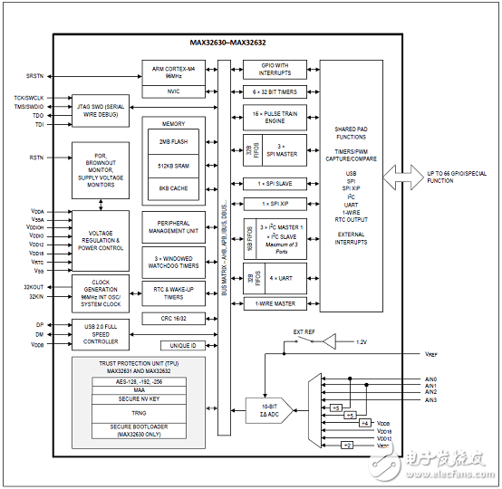
图1.MAX32631简化框图
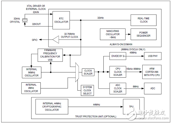
图2.MAX32630-2时钟方案
MAX32631应用:
Fitness Monitors
Portable Medical Devices
Sensor Hubs
Sports Watches
Wearable Medical Patches
评估板MAX32630 EVK
The MAX32630 and MAX32631 evaluation kits (EV kits) provide a convenient platform for evaluating the capabilities of the MAX32630–MAX32632 microcontrollers, respectively. While the MAX32630 EV kit includes a MAX32630 soldered directly to the board, the MAX32631 EV kit features a socketed MAX32631. This version can be used to evaluate the MAX32632, but contact the factory for samples. Each EV kit also provides a complete, functional system ideal for development and debugging applications. Except where stated otherwise, the following sections apply to both EV kits.
评估板MAX32630 EVK主要优势和特性:
Easily Load and Debug Code Using the Supplied Olimex Arm-USB-TINY-H JTAG Debugger Connected Through a Standard 20-Pin ARM JTAG Header
Headers for Accessing the IC’s I/O Pins and Analog Front End (AFE) Input Signals
USB Micro-B Connection to the IC’s USB Device Controller
USB Micro-B Connection to USB-UART Bridge Selectable Between the IC’s Internal UART 0 and UART 1
On-Board Bluetooth® 4.0 BLE Transceiver with Chip Antenna
评估板MAX32630 EVK包括:
EV kit board with a soldered MAX32630 (MAX32630-EVKIT#)
EV kit board with a socketed MAX32631 (MAX32631-EVKIT#)
Olimex® Arm®-USB-TINY-H JTAG debugger with JTAG ribbon cable (for connecting from debugger to EV kit header J1) and USB standard A-to-B cable (for connecting from PC to debugger)
Two standard-A to Micro-B USB cables (for connecting from a PC or stand-alone USB power supply to EV kit connectors CN1 and CN2)
MAX32630/MAX32631 EV Kit Quick Start
Hex Keys for the Socket (MAX32631 EV Kit Only)
图3.评估板MAX32630 EVK外形图
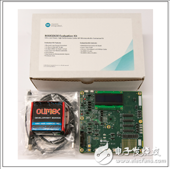
图4.评估板MAX32630 EVK套件图
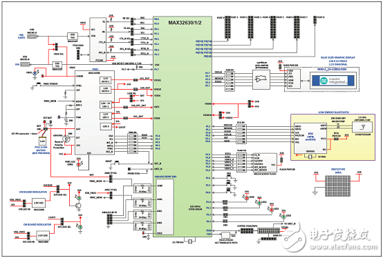
图5.评估板MAX32630 EVK框图

图6.评估板MAX32630 EVK威廉希尔官方网站 图(1)
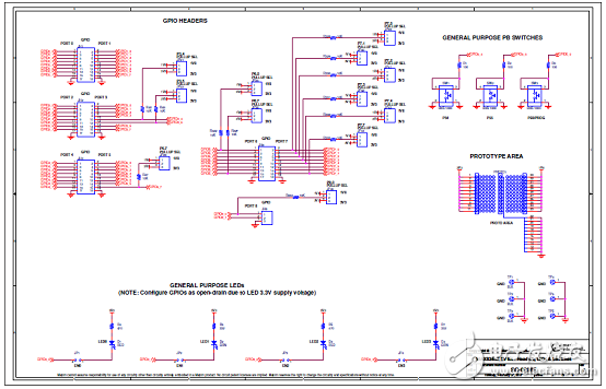
图7.评估板MAX32630 EVK威廉希尔官方网站 图(2)
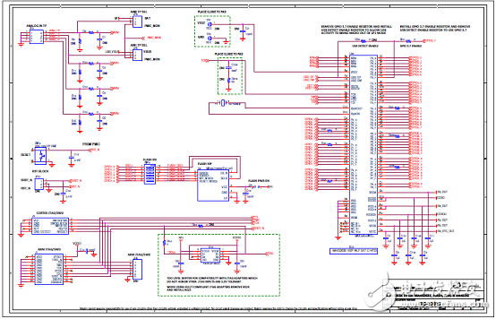
图8.评估板MAX32630 EVK威廉希尔官方网站 图(3)
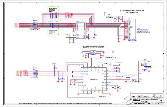
图9.评估板MAX32630 EVK威廉希尔官方网站 图(4)
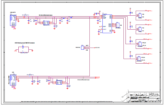
图10.评估板MAX32630 EVK威廉希尔官方网站 图(5)
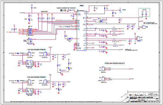
图11.评估板MAX32630 EVK威廉希尔官方网站 图(6)
评估板MAX32630 EVK材料清单:
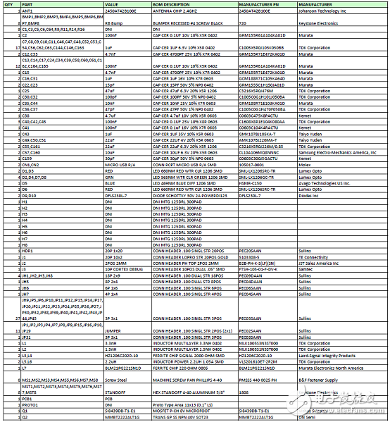
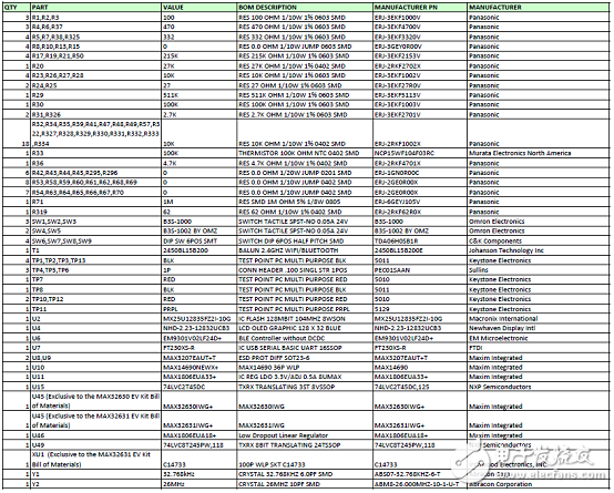
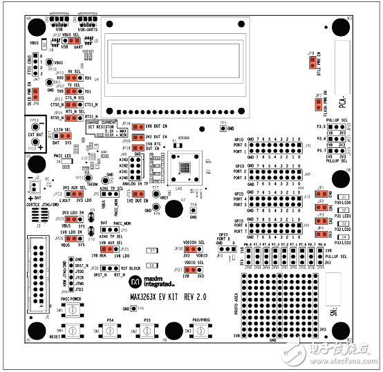
图12.评估板MAX32630 EVK默认开关设置图
详情请见:
https://datasheets.maximintegrated.com/en/ds/MAX32630-MAX32632.pdf
和https://datasheets.maximintegrated.com/en/ds/MAX32630-EVKIT-MAX32631-EVKIT.pdf
MAX32630-MAX32632.pdf
MAX32630-EVKIT-MAX32631-EVKIT.pdf
-
大数据推动可穿戴设备的发展2014-09-10 0
-
可穿戴设备开发相关攻略及主要厂商精选2015-01-04 0
-
可穿戴设备2016-01-15 0
-
低功耗蓝牙可穿戴设备创造人机交互新体验?2016-09-02 0
-
探讨可穿戴设备的未来2016-12-05 0
-
快速开发支持蓝牙的无线充电可穿戴设备2017-04-01 0
-
可穿戴设备中无需维护的电池的实现2018-10-10 0
-
ON Semiconductor真正可拓展可穿戴设备开发神器2018-11-08 0
-
智能服装拯救可穿戴设备“冷市场”?2018-11-19 0
-
可穿戴设备这么小却用处很多2019-03-20 0
-
可穿戴设备的构成和分类2019-07-10 0
-
可穿戴设备的传感器的作用2020-08-21 0
-
主流的几家可穿戴设备芯片供应商2021-02-03 0
-
面向可穿戴设备市场的温度检测参考设计2022-09-14 0
-
基于ARM Cortex-M4F内核的MAX32630和MAX32631微控制器2020-07-11 668
全部0条评论

快来发表一下你的评论吧 !

