
DS2151, DS2153 Interfacing to
通信设计应用
63人已加入
描述
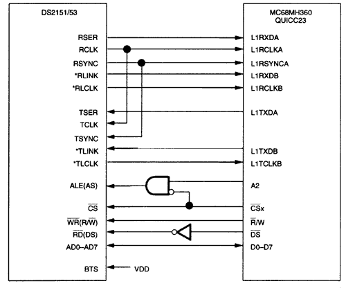
Abstract: Application Note 304 provides a logical diagram of the interface of the Dallas Semiconductor/Maxim DS2151 T1 single chip transceiver (SCT) and DS2153 E1 SCT to the Motorola MC68MH360 QUICC32.
Interconnections between the DS2151 or DS2153 and the Motorola MC68MH360 (QUICC32) are shown in Figure 1. The MC68MH360 can be configured as an HDLC controller implementing protocols such as LAPD for both D channel and the FDL. In the configuration Shown, TDM channel A is used for timeslots 0-23 (T1) or 0-31 (E1) and TDM channel B is used for the FDL. For more information see the application note on Interfacing to a Non-Multiplex Bus.

*HDLC on the FDL can be implemented either by the second serial input (TDM CHANNEL B) or via the port by the host processor (CPU32 internal to the QUICC32).
打开APP阅读更多精彩内容
Interconnections between the DS2151 or DS2153 and the Motorola MC68MH360 (QUICC32) are shown in Figure 1. The MC68MH360 can be configured as an HDLC controller implementing protocols such as LAPD for both D channel and the FDL. In the configuration Shown, TDM channel A is used for timeslots 0-23 (T1) or 0-31 (E1) and TDM channel B is used for the FDL. For more information see the application note on Interfacing to a Non-Multiplex Bus.

*HDLC on the FDL can be implemented either by the second serial input (TDM CHANNEL B) or via the port by the host processor (CPU32 internal to the QUICC32).
DS2151, DS2153 Notes:
- Other signals affecting operation of device are not shown.
- Example circuit has RSYNC in output mode.
MC68360 Notes:
- Other signals affecting operation of device are not shown.
- Use SI mode register t
- Set up transmit and receive frame sync delays (0-3 clocks) to mask the F-Bit in T1 applications. RFSDA = 1 for DS2151, 0 for DS2153.
- Set clock edges for transmit on rising edge and receive on falling edge. CEA = CEB = 0.
- In the above example, TDM channel A has a common transmit/receive clock and sync. CRTA = 1.
- Use the TIMESLOT ASSIGNER to ignore Timeslot 0 for the DS2153.
声明:本文内容及配图由入驻作者撰写或者入驻合作网站授权转载。文章观点仅代表作者本人,不代表电子发烧友网立场。文章及其配图仅供工程师学习之用,如有内容侵权或者其他违规问题,请联系本站处理。
举报投诉
- 相关推荐
- DS2151
-
DS2151, DS2152, DS2153, DS21542009-04-20 875
-
DS2141A, DS2143, DS2151, DS2152009-04-20 659
-
DS2151, DS2153 Interfacing to2009-04-20 794
-
DS2151, DS2153 Creating a T1/E2009-04-20 1100
-
DS2141A, DS2143, DS2151 and DS2009-04-29 853
-
DS2151,DS2153连接的ADSP-2181-DS212009-04-29 849
-
ds2141a,ds2143,ds2151,ds2153接口的西门子peb20452017-04-10 813
-
ds2151,ds2153 interfacing to the mc68mh360 quicc322017-04-10 776
-
ds2151,ds2153到AT&T T7270接口2017-04-11 851
全部0条评论

快来发表一下你的评论吧 !

