

High-Speed I²C for the MA
通信设计应用
63人已加入
描述
Abstract: This application note provides a much-needed working high-speed I2C example. The application note shows an application circuit and provides all the firmware required to interface the MAXQ2000 microcontroller (MAXQ20 core) to the MAX1239 for a conversion rate of 91ksps. The example firmware was developed using the MAX-IDE Version 1.0.
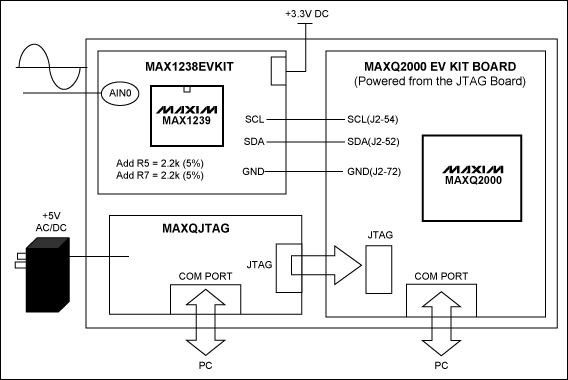
Figure 1. A simplified system block diagram.
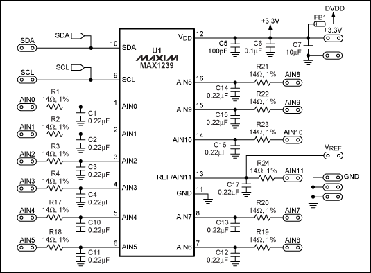
Figure 2. Modified MAX1238 EV kit schematic using a MAX1239.
The pinout of the MAX1239 allows easy isolation of the analog circuitry from the digital circuitry; the analog circuitry is grouped together on the left side of the board, and the digital circuitry is grouped together on the right side of the board. Keep this in mind when connecting the two boards together. Connect J2-52 (SDA) on the MAXQ2000 EV kit board to the SDA pad on the MAX1238 EV kit. Similarly, connect J2-54 (SCL) to the SCL pad. The grounds of both boards must be connected together. In addition, R5 and R7 both have to be populated with 2.2kΩ 5% resistors. The MAX1238 EV kit already has 47kΩ I²C pullup resistors and the MAXQ2000 EV kit has 10kΩ I²C pullup resistors. Adding R5 and R7 will provide approximately 1.6kΩ of pullup resistance on the I²C bus.
The MAXQ2000 EV kit contains a complete set of hardware, software, sample code, and documentation needed to start designing with the MAXQ2000. Schematics for the MAXQ2000 EV kit are available in the data sheet.
The main source file is hsi2c.asm, and it was written in assembly to optimize the timing of the HS-mode I²C interface. The source code does the following things:
The hsi2c.asm file defaults to the slave address of the MAX1239EEE or MAX1239EEE+. The firmware must be customized for each different part in the family. For example, follow the two steps below when using the MAX1239KEEE, MAX1239KEEE+, MAX1239LEEE, MAX1239LEEE+, MAX1239MEEE, or MAX1239MEEE+:
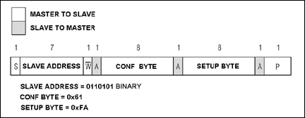
Figure 3. FS-mode two-byte write operation.
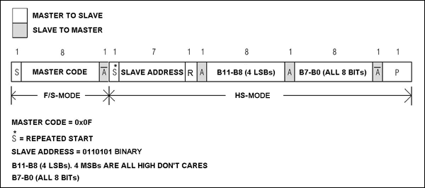
Figure 4. HS-mode receive operation.
Figures 5 through Figure 16 are scope shots of the FS-mode (Figure 3) and HS-mode (Figure 4) I²C frames implemented in this application note. Channel 1 is SCL and Channel 2 is SDA on all scope shots.
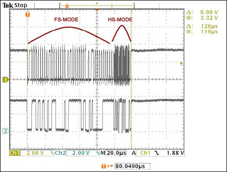
Figure 5. A complete frame of all the I²C communication (FS-mode and HS-mode operations).
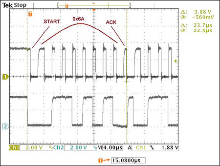
Figure 6. FS-mode operation, Byte1 (start + Addr = 0x6A + ACK).
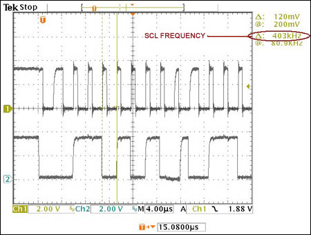
Figure 7. The SCL clock frequency in FS mode is approximately 400kHz.
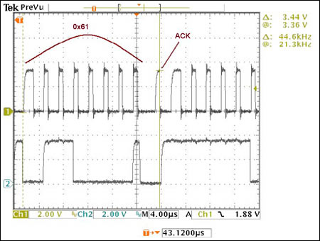
Figure 8. FS-mode operation, Byte2 (conf byte = 0x61 + ACK).
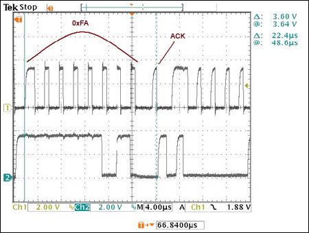
Figure 9. FS-mode operation, Byte3 (setup byte = 0xFA + ACK).
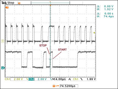
Figure 10. FS-mode operation, stop and start of next operation (stop and start).
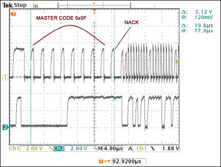
Figure 11. FS-mode operation, Byte4 (master code = 0x0F + NACK).
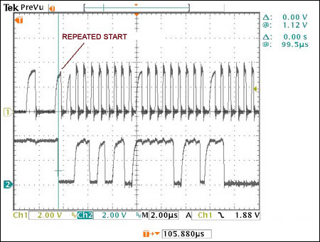
Figure 12. HS-mode operation, repeated start.
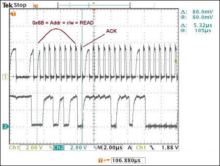
Figure 13. HS-mode operation, Byte5 (Addr = 0x6B + ACK).
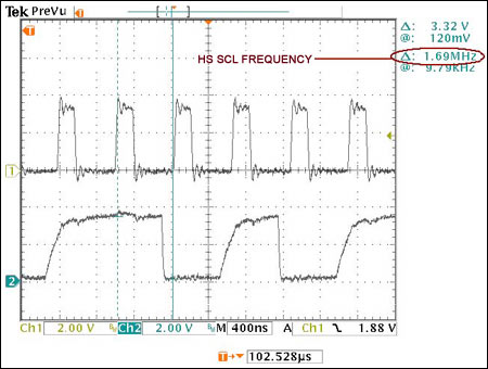
Figure 14. The SCL clock frequency in HS mode is approximately 1.7MHz.
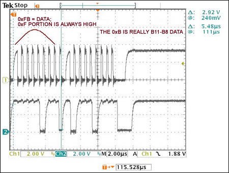
Figure 15. HS-mode operation, Byte6 (data = 0xFB + ACK).
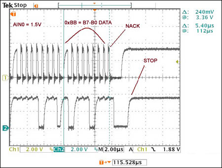
Figure 16. HS-mode operation, Byte7 (data = 0xBB + NACK + FS-Stop).
The specification for high-speed I²C has existed since January 2000. Nonetheless, few, if any microcontrollers are available today with an internal high-speed I²C peripheral. This is an unfortunate situation since several devices, such as ADCs, DACs, CODECs, and even power supplies, are being designed to support the high-speed I²C interface. This application note provides a much-needed working, high-speed I²C example.
Download: Source Code
打开APP阅读更多精彩内容
MAX1239 Overview
The MAX1239 is a 12-channel, 12-bit, low-power ADC featuring a 1.7MHz high-speed I²C-compatible serial interface. The MAX1239 supports both Fast/Standard mode (FS mode at 400kHz) and High-Speed mode (HS mode at 1.7MHz) with conversion rates up to 94.4ksps. HS mode is required to achieve conversion rates from 26ksps to 94.4ksps. External clock mode is required for conversion rates from 40ksps to 94.4ksps.Hardware Overview
A simplified system block diagram is shown in Figure 1. The application circuit utilizes two evaluation (EV) kits: the MAX1238EVKIT with an installed MAX1239 (instead of a MAX1238), and a MAXQ2000-KIT. The MAX1239 was selected because of the digital-logic voltage range. The MAXQ2000 microcontroller's general-purpose input/output (GPIO) ports only accept up to +3.3V; using level translators with high-speed I²C would have made the circuit overly complicated. The MAXQ2000 is not present on the MAX1238 EV kit board, so it was added to the system by connecting SCL, SDA, and GND on both boards. In addition, it is very important to apply +3.3V (instead of +5V) to VDD on the MAX1238 EV kit board. Order a free sample of the MAX1239EEE or MAX1239EEE+ and solder it onto the MAX1238 EV kit. The modified MAX1238 EV kit schematic is shown in Figure 2.
Figure 1. A simplified system block diagram.

Figure 2. Modified MAX1238 EV kit schematic using a MAX1239.
The pinout of the MAX1239 allows easy isolation of the analog circuitry from the digital circuitry; the analog circuitry is grouped together on the left side of the board, and the digital circuitry is grouped together on the right side of the board. Keep this in mind when connecting the two boards together. Connect J2-52 (SDA) on the MAXQ2000 EV kit board to the SDA pad on the MAX1238 EV kit. Similarly, connect J2-54 (SCL) to the SCL pad. The grounds of both boards must be connected together. In addition, R5 and R7 both have to be populated with 2.2kΩ 5% resistors. The MAX1238 EV kit already has 47kΩ I²C pullup resistors and the MAXQ2000 EV kit has 10kΩ I²C pullup resistors. Adding R5 and R7 will provide approximately 1.6kΩ of pullup resistance on the I²C bus.
The MAXQ2000 EV kit contains a complete set of hardware, software, sample code, and documentation needed to start designing with the MAXQ2000. Schematics for the MAXQ2000 EV kit are available in the data sheet.
Firmware Overview
The example firmware was developed using the free MAX-IDE Version 1.0. Download the latest version of the MAX-IDE.The main source file is hsi2c.asm, and it was written in assembly to optimize the timing of the HS-mode I²C interface. The source code does the following things:
a) Initializes the MAXQ2000's UART for 8-N-1 at 115.2kbpsThe example assembly program collects samples from the MAX1239 by bit-banging a HS-mode I²C interface on the MAXQ2000's GPIO ports. The MAXQ2000's 16MHz system clock allows the bit-banged HS-mode I²C interface to run up to 1.7MHz.
b) Initializes the MAX1239 CONF BYTE for single-ended channel AIN0
c) Initializes the MAX1239 SETUP BYTE for the internal reference, external clock, and unipolar operation
d) Initializes the MAX1239 for I²C HS mode
e) Reads back 12-bit samples from the MAX1239 in I²C HS mode
f) Transmits the 12-bit samples over the serial port
The hsi2c.asm file defaults to the slave address of the MAX1239EEE or MAX1239EEE+. The firmware must be customized for each different part in the family. For example, follow the two steps below when using the MAX1239KEEE, MAX1239KEEE+, MAX1239LEEE, MAX1239LEEE+, MAX1239MEEE, or MAX1239MEEE+:
- Edit the I2C_ADDR define statements to reflect the I²C address of the part used. These variables are required to be the compliment of the actual address. For example, an address of 0111 111 (r/w) needs to be encoded as:
I2C_ADDR7 equ 1
I2C_ADDR6 equ 0
I2C_ADDR5 equ 0
I2C_ADDR4 equ 0
I2C_ADDR3 equ 0
I2C_ADDR2 equ 0
I2C_ADDR1 equ 0 - The source code expects a 16MHz system clock to be used (MAXQ2000 crystal).

Figure 3. FS-mode two-byte write operation.

Figure 4. HS-mode receive operation.
Figures 5 through Figure 16 are scope shots of the FS-mode (Figure 3) and HS-mode (Figure 4) I²C frames implemented in this application note. Channel 1 is SCL and Channel 2 is SDA on all scope shots.

Figure 5. A complete frame of all the I²C communication (FS-mode and HS-mode operations).

Figure 6. FS-mode operation, Byte1 (start + Addr = 0x6A + ACK).

Figure 7. The SCL clock frequency in FS mode is approximately 400kHz.

Figure 8. FS-mode operation, Byte2 (conf byte = 0x61 + ACK).

Figure 9. FS-mode operation, Byte3 (setup byte = 0xFA + ACK).

Figure 10. FS-mode operation, stop and start of next operation (stop and start).

Figure 11. FS-mode operation, Byte4 (master code = 0x0F + NACK).

Figure 12. HS-mode operation, repeated start.

Figure 13. HS-mode operation, Byte5 (Addr = 0x6B + ACK).

Figure 14. The SCL clock frequency in HS mode is approximately 1.7MHz.

Figure 15. HS-mode operation, Byte6 (data = 0xFB + ACK).

Figure 16. HS-mode operation, Byte7 (data = 0xBB + NACK + FS-Stop).
The specification for high-speed I²C has existed since January 2000. Nonetheless, few, if any microcontrollers are available today with an internal high-speed I²C peripheral. This is an unfortunate situation since several devices, such as ADCs, DACs, CODECs, and even power supplies, are being designed to support the high-speed I²C interface. This application note provides a much-needed working, high-speed I²C example.
Download: Source Code
声明:本文内容及配图由入驻作者撰写或者入驻合作网站授权转载。文章观点仅代表作者本人,不代表电子发烧友网立场。文章及其配图仅供工程师学习之用,如有内容侵权或者其他违规问题,请联系本站处理。
举报投诉
- 相关推荐
- MAX1239
-
High-Speed Interconnect -高速接口I2009-03-23 735
-
High-Speed Differential Signal2009-05-14 468
-
MAX7360,pdf datasheet (I²;2009-06-20 635
-
High-Speed Audio Ripping,Encod2009-09-30 692
-
DS1340, DS1340C I²;C实时时钟,带2008-09-22 1385
-
DS3514 I²;C Gamma and VCOM2008-10-24 1198
-
How to Use the DS2482 I²;C2008-12-18 1496
-
I²;C总线的验证及实现--Proven Imple2009-01-22 2147
-
Comparing the I²;C Bus to2009-04-30 827
-
如何使用I²;C接口的DS2482 1-Wire主控2009-05-09 3465
-
Maxim推出I²;C兼容、多通道8/10/12位A2009-11-13 889
-
欧司朗推出采用I²;C数字输出的环境光度传感器2009-11-18 555
-
Maxim推出集成振荡器的微型SPI/I²;C UA2010-01-18 617
-
MAX11835 带有I²;C接口的触觉反馈压电控制2010-02-05 1036
全部0条评论

快来发表一下你的评论吧 !

