

与Microchip PICmicro微控制器之间的1-Wi
通信设计应用
63人已加入
描述
摘要:Dallas Semiconductor的产品中有些包含了1-Wire®通信接口,适用于不同系统。这些系统中可能需要与著名的Microchip PICmicro® (PIC)接口。为方便1-Wire器件与PIC微控制器的接口,本应用笔记给出了用于PIC微控制器的1-Wire软件例程,时序说明和相关资料。本应用还提供一个包含了所有1-Wire子程序的文件,所提供的汇编程序是针对PIC16F628读取高精度Li+电池监视器DS2761的数据编写的。
第二个宏指令OW_LO的功能就是把DQ强制变为低电平。首先选择数据存储器的bank 0,这样PORTB寄存器就被寻址。PORTB寄存器是数据存储器,当设置作为输出时,它包含了那些TRISB中配置为输出引脚的强制输出值。
将PORTB的DQ位清零,这样引线就强制变为低电平。最后选择数据存器的bank 1,PORTB寄存器的DQ位清零,使其用作输出驱动。和其它一样,宏指令以选择数据存储器的bank 0结束。
最后的宏指令WAIT用于产生1-Wire信令所需要的延时。WAIT可产生5µs的整数倍的延时。在这个宏指令中,先简单计算出所需的5µs延时的整倍数,然后在WAIT5U做相应次数的循环。WAIT5U子程序将在下一节讨论。对于WAIT内的每一条指令,所用处理时间都进行了注释,以方便理解延时是怎样实现的
表1. 标准速率下1-Wire接口定时要求
1-Wire通信的所有过程都是从主机发的一个复位脉冲开始,随后跟着从机的应答检测脉冲(presence detect pulse)。 图1对这个事务处理进行了阐述。初始化序列可通过PIC发出,很简单,对应的汇编代码如图1所示。初始化、读操作、写操作的时序参数已在表1中列出。在本文的后面部分也将以这些参数为参考。
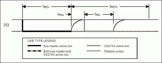
图1. 1-Wire的初始化序列
1-Wire通信需要的另外一个子程序就是DSTXBYTE,用于向1-Wire从器件发送数据。这个子程序的PIC代码如图2所示。这个子程序需要和WREG寄存器中要发送的数据一起调用。首先将要发送的数据立即放入IOBYTE寄存器,随后将COUNT寄存器初始化为8,以用来对要在DQ口线上发送的位进行计数。从DSTXLP开始,PIC才送出数据。开始时不管发送的电平是高是低,DQ引脚都变低电平3µs,这样就可满足tLOW1的要求。随后IOBYTE的LSB移位至CARRY位,然后检测是0还是1。如果CARRY是1,TRISB的DQ位置位,引脚变为高阻态,线路被上拉电阻拉为高电平。如果CARRY是0,线路就维持低电平。之后又引入60µs的延时以便在tLOW0在最小值时仍能正常工作。60µs的等待之后,该引脚变为高阻态,之后又是2µs的附加延时以便上拉电阻复原。最后COUNT减1。如果COUNT寄存器的值成了0,表示所有的数据已经发送完毕,子程序结束。如果COUNT寄存器的值不是0,就从DSTXLP开始继续发送下一位数据。关于如何在程序中写入0或写入1参见图2。
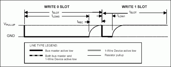
图2. 1-Wire写操作时序
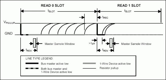
图3. 1-Wire读时隙
打开APP阅读更多精彩内容
引言
Microchip公司的PICmicro微控制器(PIC)已经成为低功耗、低成本系统解决方案的主流选择。这些微处理器有多个通用输入输出引脚(GPIO),通过对这些引脚进行简单组合就可实现Dallas Semiconductor的1-Wire协议,1-Wire协议可使包括电池管理、温度管理、存储器、iButton®在内的多种Dallas Semiconductor器件协调工作。本应用笔记给出了基于PIC16F628的1-Wire通信子程序,并对其时序及其它相关内容进行了详细介绍。为方便起见,所有的时钟频率假定为4MHz。大家知道这个频率也是许多PIC的内部时钟频率。附录A是这些所有子程序都包含的一个文件,附录B是PIC16F628从高精度锂电池监视器DS2761读取数据的一段汇编语言代码。这里要说明的一点是,本应用笔记仅仅适合于常规速度的1-Wire通信。通用宏指令
主机端1-Wire协议的实现,GPIO只需要两个状态即可,即高阻态和逻辑低电平,下面这一小段汇编程序就是用来实现这个功能的。PIC16F628有两组GPIO端口:PORTA和PORTB,其中任何一组都可以用来完成1-Wire通信。在这个例子中,选择了PORTB,同时在汇编代码中也配置了一个常数DQ,用于设定采用PORTB的哪一位来作为1-Wire引脚。在代码的自始至终,该位被简称为DQ。在威廉希尔官方网站 外面,这个引脚要通过一个上拉电阻接至电源正端。 OW_HIZ:MACRO
;Force the DQ line into a high impedance state.
BSF STATUS,RP0 ; Select Bank 1 of data memory
BSF TRISB, DQ ; Make DQ pin High Z
BCF STATUS,RP0 ; Select Bank 0 of data memory
ENDM
OW_LMACRO
;Force the DQ line to a logic low.
BCF STATUS,RP0 ; Select Bank 0 of data memory
BCF PORTB, DQ ; Clear the DQ bit
BSF STATUS,RP0 ; Select Bank 1 of data memory
BCF TRISB, DQ ; Make DQ pin an output
BCF STATUS,RP0 ; Select Bank 0 of data memory
ENDM
这两段代码都是作为宏指令来编写的。把它们写成宏指令,在汇编源代码中通过一个宏指令调用即可自动插入这些代码,这样就减少了代码重写的次数。第一个宏指令OW_HIZ的功能就是把DQ强制变为高阻态。由于TRISB寄存器位于数据存储器的bank 1,所以第一步就是选择数据存器的bank 1。接着通过把TRISB寄存器的DQ位置位,使DQ输出驱动器变为高阻态。代码的最后一行变回到数据存储器的bank 0,最后一行不是必需的,但这里还是加进去了,以便所有的宏指令和功能调用之后数据存储器都处在一个确定的状态。第二个宏指令OW_LO的功能就是把DQ强制变为低电平。首先选择数据存储器的bank 0,这样PORTB寄存器就被寻址。PORTB寄存器是数据存储器,当设置作为输出时,它包含了那些TRISB中配置为输出引脚的强制输出值。
将PORTB的DQ位清零,这样引线就强制变为低电平。最后选择数据存器的bank 1,PORTB寄存器的DQ位清零,使其用作输出驱动。和其它一样,宏指令以选择数据存储器的bank 0结束。
最后的宏指令WAIT用于产生1-Wire信令所需要的延时。WAIT可产生5µs的整数倍的延时。在这个宏指令中,先简单计算出所需的5µs延时的整倍数,然后在WAIT5U做相应次数的循环。WAIT5U子程序将在下一节讨论。对于WAIT内的每一条指令,所用处理时间都进行了注释,以方便理解延时是怎样实现的
      WAIT:MACRO TIME
      ;Delay for TIME µs.
      ;Variable time must be in multiples of 5µs.
             MOVLW (TIME/5) - 1                 ;1µs to process
             MOVWF TMP0                         ;1µs to process
             CALL WAIT5U                        ;2µs to process
             ENDM
1-Wire通用子程序
为了保证通信成功,1-Wire定时协议中有一些必须遵守的特殊定时限制。为方便产生特殊的延时,可采用子程序WAIT5U来产生5µs的延时。这个子程序如下: WAIT5U:
;This takes 5µs to complete
NOP ;1µs to process
NOP ;1µs to process
DECFSZ TMP0,F ;1µs if not zero or 2µs if zero
GOTO WAIT5U ;2µs to process
RETLW 0 ;2µs to process
这个子程序和WAIT宏指令一起使用,即可产生常用的延时。例如如果需要40µs的延时,就调用WAIT 0.40。先运行WAIT的前3行,产生4µs的延时,然后运行6次WAIT5U的前4行,每次产生5µs的延时,总延时为30µs,最后一圈的WAIT5U需要6µs,然后就返回到WAIT宏指令,这样总的处理时间就是30 + 4 + 6 = 40µs。表1. 标准速率下1-Wire接口定时要求
| 2.5V < VDD < 5.5V, TA = -20°C to 70°C | |||||
| Parameter | Symbol | Min | Typ | Max | Units |
| Time Slot | tSLOT | 60 | 120 | µs | |
| Recovery Time | tREC | 1 | µs | ||
| Write 0 Low Time | tLOW0 | 60 | 120 | µs | |
| Write 1 Low Time | tLOW1 | 1 | 15 | µs | |
| Read Data Valid | tRDV | 15 | µs | ||
| Reset Time High | tRSTH | 480 | µs | ||
| Reset Time Low | tRSTL | 480 | 960 | µs | |
| Presence Detect High | tPDH | 15 | 60 | µs | |
| Presence Detect Low | tPDL | 60 | 240 | µs | |
1-Wire通信的所有过程都是从主机发的一个复位脉冲开始,随后跟着从机的应答检测脉冲(presence detect pulse)。 图1对这个事务处理进行了阐述。初始化序列可通过PIC发出,很简单,对应的汇编代码如图1所示。初始化、读操作、写操作的时序参数已在表1中列出。在本文的后面部分也将以这些参数为参考。
图1. 1-Wire的初始化序列
      OW_RESET:
             OW_HIZ                             ; Start with the line high
             CLRF      PDBYTE                   ; Clear the PD byte
             OW_LO
             WAIT      .500                     ; Drive Low for 500µs
             OW_HIZ
             WAIT      .70                      ; Release line and wait 70µs for PD Pulse
             BTFSS     PORTB,DQ                 ; Read for a PD Pulse
             INCF      PDBYTE,F                 ; Set PDBYTE to 1 if get a PD Pulse
             WAIT      .430                     ; Wait 430µs after PD Pulse
             RETLW     0
OW_RESET子程序从确保DQ引脚处于高阻态开始,这样就可以通过上拉电阻把DQ拉为高电平。随后清PDBYTE寄存器,这样就为随后的在位检测脉冲做好了准备。之后DQ变为低电平500µs,这就满足了表1中tRSTL参数的要求,同时还留出了20µs额外的缓冲时间。把这个引脚变为低电平之后,又回到高阻态,在开始读取在位检测脉冲之前又加入一70µs的延时。这个70µs的延时可以保证无论tPDL、 tPDH如何变化,PIC总能在有效的时间进行取样。一旦读到在位检测脉冲,PDBYTE寄存器就设置为已读到逻辑状态值。DQ引脚再保持高阻态430µs,以保证满足tRSTH的要求,还可留出20µs额外的缓冲时间。1-Wire通信需要的另外一个子程序就是DSTXBYTE,用于向1-Wire从器件发送数据。这个子程序的PIC代码如图2所示。这个子程序需要和WREG寄存器中要发送的数据一起调用。首先将要发送的数据立即放入IOBYTE寄存器,随后将COUNT寄存器初始化为8,以用来对要在DQ口线上发送的位进行计数。从DSTXLP开始,PIC才送出数据。开始时不管发送的电平是高是低,DQ引脚都变低电平3µs,这样就可满足tLOW1的要求。随后IOBYTE的LSB移位至CARRY位,然后检测是0还是1。如果CARRY是1,TRISB的DQ位置位,引脚变为高阻态,线路被上拉电阻拉为高电平。如果CARRY是0,线路就维持低电平。之后又引入60µs的延时以便在tLOW0在最小值时仍能正常工作。60µs的等待之后,该引脚变为高阻态,之后又是2µs的附加延时以便上拉电阻复原。最后COUNT减1。如果COUNT寄存器的值成了0,表示所有的数据已经发送完毕,子程序结束。如果COUNT寄存器的值不是0,就从DSTXLP开始继续发送下一位数据。关于如何在程序中写入0或写入1参见图2。
图2. 1-Wire写操作时序
      DSTXBYTE:                                 ; Byte to send starts in W
             MOVWF     IOBYTE                   ; We send it from IOBYTE
             MOVLW     .8
             MOVWF     COUNT                    ; Set COUNT equal to 8 to count the bits
      DSTXLP:
             OW_LO
             NOP
             NOP
             NOP                                ; Drive the line low for 3µs
             RRF        IOBYTE,F
             BSF        STATUS,RP0              ; Select Bank 1 of data memory
             BTFSC      STATUS,C                ; Check the LSB of IOBYTE for 1 or 0
             BSF        TRISB,DQ                ; HiZ the line  if LSB is 1
             BCF        STATUS,RP0              ; Select Bank 0 of data memory
             WAIT      .60                      ; Continue driving line for 60µs
             OW_HIZ                             ; Release the line for pullup
             NOP
             NOP                                ; Recovery time of 2µs
             DECFSZ    COUNT,F                  ; Decrement the bit counter
             GOTO      DSTXLP
             RETLW     0
1-Wire通信的最后一个子程序是DSRXBYTE,主要功能是从从器件接收信息,其代码如图3所示。在DQ有所动作之前首先把COUNT寄存器初始化为8,表示要接收的位数。开始时DSRXLP首先把DQ引脚变为低电平,向从器件发出信号,表示已经做好接收数据的准备。该线保持低电平6µs,通过将DQ线置为高阻态来释放口线,随后PIC在采样数据线之前要再等待4µs。当口线电平变低之后,在OW_LO存在1行代码,在OW_HIZ之中存在3行代码。一行代码的处理时间为1µs,所有的时间加在一起就是1 + 6 + 3 + 4 = 14µs,刚好比15µs的tRDV低。PORTB读取之后,DQ位被屏蔽,该寄存器进行加法运算直到255,强制CARRY位去镜像DQ位,然后CARRY位移位至保存接收数据的IOBYTE。一旦这个字节被存储起来,就需要再引入50µs的延时,以保证满足tSLOT的要求。最后检查是判断COUNT寄存器是否为零。如果为零,则表明已读完8位,退出子程序;否则,转到DSRXLP处重复这个循环。读0和读1的过程如图3所示。 图3. 1-Wire读时隙
DSRXBYTE: ; Byte read is stored in IOBYTE
MOVLW .8
MOVWF COUNT ; Set COUNT equal to 8 to count the bits
DSRXLP:
OW_LO
NOP
NOP
NOP
NOP
NOP
NOP ; Bring DQ low for 6µs
OW_HIZ
NOP
NOP
NOP
NOP ; Change to HiZ and Wait 4µs
MOVF PORTB,W ; Read DQ
ANDLW 1<
小结
Microchip微控制器的PICmicro可以很容易地实现Dallas Semiconductor的1-Wire通信协议。1-Wire数据传输的实现,只需要GPIO的两个状态。PIC有多个GPIO,因此很容易就可完成这样的工作。1-Wire通信有3个基本的字程序:初始化、读数据、写数据。本文对这3个子程序完整详细地作了介绍,用它可以完成常规速度的1-Wire通信,这样就可使PIC与Dallas Semiconductor的任何1-Wire器件接口。文后的附录A是一个3个子程序的传统头文件,附录B则是PIC16F628与高精度锂电池监视器DS2761相连的一段汇编小程序。
附录A:1-Wire包含FILE (1W_16F6X.INC)
; *******************************************************
;
; Dallas 1-Wire Support for PIC16F628
;
; Processor has 4MHz clock and 1µs per instruction cycle.
;
; *******************************************************
; *******************************************************
; Dallas Semiconductor 1-Wire MACROS
; *******************************************************
OW_HIZ:MACRO
BSF STATUS,RP0 ; Select Bank 1 of data memory
BSF TRISB, DQ ; Make DQ pin High Z
BCF STATUS,RP0 ; Select Bank 0 of data memory
ENDM
; --------------------------------------------------------
OW_LMACRO
BCF STATUS,RP0 ; Select Bank 0 of data memory
BCF PORTB, DQ ; Clear the DQ bit
BSF STATUS,RP0 ; Select Bank 1 of data memory
BCF TRISB, DQ ; Make DQ pin an output
BCF STATUS,RP0 ; Select Bank 0 of data memory
ENDM
; --------------------------------------------------------
WAIT:MACRO TIME
;Delay for TIME µs.
;Variable time must be in multiples of 5µs.
MOVLW (TIME/5)-1 ;1µs
MOVWF TMP0 ;1µs
CALL WAIT5U ;2µs
ENDM
; *******************************************************
; Dallas Semiconductor 1-Wire ROUTINES
; *******************************************************
WAIT5U:
;This takes 5µS to complete
NOP ;1µs
NOP ;1µs
DECFSZ TMP0,F ;1µs or 2µs
GOTO WAIT5U ;2µs
RETLW 0 ;2µs
; --------------------------------------------------------
OW_RESET:
OW_HIZ ; Start with the line high
CLRF PDBYTE ; Clear the PD byte
OW_LO
WAIT .500 ; Drive Low for 500µs
OW_HIZ
WAIT .70 ; Release line and wait 70µs for PD Pulse
BTFSS PORTB,DQ ; Read for a PD Pulse
INCF PDBYTE,F ; Set PDBYTE to 1 if get a PD Pulse
WAIT .400 ; Wait 400µs after PD Pulse
RETLW 0
; --------------------------------------------------------
DSRXBYTE: ; Byte read is stored in IOBYTE
MOVLW .8
MOVWF COUNT ; Set COUNT equal to 8 to count the bits
DSRXLP:
OW_LO
NOP
NOP
NOP
NOP
NOP
NOP ; Bring DQ low for 6µs
OW_HIZ
NOP
NOP
NOP
NOP ; Change to HiZ and Wait 4µs
MOVF PORTB,W ; Read DQ
ANDLW 1<
附录B:PIC16F628至DS2761汇编代码(PIC_2_1W.ASM)
; *******************************************
;
; Dallas Semiconductor PIC code
;
; This code will interface a PIC16F628 microcontroller to
; a DS2761 High-Precision Li+ Battery Monitor
;
; *******************************************;
;
; VCC
; ^
; |
; |
; /
; \ Rpup
; /
; \
; |
; 16F628 | DS2761
; RB1 (pin 7) ------------------------------ DQ (pin 7)
;
; *******************************************;
;---------------------------------------------------------
; List your processor here.
list p=16F628
; Include the processor header file here.
#include
;---------------------------------------------------------
; Assign the PORTB with Constants
constant DQ=1 ; Use RB1 (pin7) for 1-Wire
;--------------------------------------------------------
; These constants are standard 1-Wire ROM commands
constant SRCHROM=0xF0
constant RDROM=0x33
constant MTCHROM=0x55
constant SKPROM=0xCC
;---------------------------------------------------------
; These constants are used throughout the code
cblock 0x20
IOBYTE
TMP0 ; Address 0x23
COUNT ; Keep track of bits
PICMSB ; Store the MSB
PICLSB ; Store the LSB
PDBYTE ; Presence Detect Pulse
endc
;---------------------------------------------------------
; Setup your configuration word by using __config.
; For the 16F628, the bits are:
; CP1,CP0,CP1,CP0,N/A, CPD, LVP, BODEN, MCLRE, FOSC2, PWRTE, WDTE, FOSC1, FOSC0
; CP1 and CP0 are the Code Protection bits
; CPD: is the Data Code Protection Bit
; LVP is the Low Voltage Programming Enable bit
; PWRTE is the power-up Timer enable bit
; WDTE is the Watchdog timer enable bit
; FOSC2, FOSC1 and FOSC0 are the oscillator selection bits.
; CP disabled, LVP disabled, BOD disabled, MCLR enabled, PWRT disabled, WDT disabled, INTRC I/O oscillator
; 11111100111000
__config 0x3F38
;---------------------------------------------------------
; Set the program origin for subsequent code.
org 0x00
GOTO SETUP
NOP
NOP
NOP
GOTO INTERRUPT ; PC 0x04...INTERRUPT VECTOR!
;---------------------------------------------------------
INTERRUPT:
SLEEP
;---------------------------------------------------------
; Option Register bits
; ____
; RBPU,INTEDG,TOCS,TOSE,PSA,PS2,PS1,PS0
; 7=PORTB Pullup Enable, 6=Interrupt Edge Select, 5=TMR0 Source,
; 4=TMR0 Source Edge, 3=Prescaler Assign, 2-0=Prescaler Rate Select
; 11010111
; PORTB pullups disabled,rising edge,internal,hightolow,TMR0,1:256
SETUP:
BCF STATUS,RP1
BSF STATUS,RP0 ; Select Bank 1 of data memory
MOVLW 0xD7
MOVWF OPTION_REG
BCF STATUS,RP0 ; Select Bank 0 of data memory
;---------------------------------------------------------
BCF INTCON,7 ; Disable all interrupts.
;---------------------------------------------------------
GOTO START
;---------------------------------------------------------
; Include the 1-Wire communication routines and macros
#INCLUDE 1w_16f6x.inc
;---------------------------------------------------------
START:
;---------------------------------------------------------
GET_TEMP:
CALL OW_RESET ; Send Reset Pulse and read for Presence Detect Pulse
BTFSS PDBYTE,0 ; 1 = Presence Detect Detected
GOTO NOPDPULSE
MOVLW SKPROM
CALL DSTXBYTE ; Send Skip ROM Command (0xCC)
MOVLW 0x69
CALL DSTXBYTE ; Send Read Data Command (0x69)
MOVLW 0x0E
CALL DSTXBYTE ; Send the DS2761 Current Register MSB address (0x0E)
CALL DSRXBYTE ; Read the DS2761 Current Register MSB
MOVF IOBYTE,W
MOVWF PICMSB ; Put the Current MSB into file PICMSB
CALL DSRXBYTE ; Read the DS2761 Current Register LSB
MOVF IOBYTE,W
MOVWF PICLSB ; Put the Current LSB into file PICLSB
CALL OW_RESET
NOPDPULSE: ; Add some error processing here!
SLEEP ; Put PIC to sleep
;---------------------------------------------------------
end
声明:本文内容及配图由入驻作者撰写或者入驻合作网站授权转载。文章观点仅代表作者本人,不代表电子发烧友网立场。文章及其配图仅供工程师学习之用,如有内容侵权或者其他违规问题,请联系本站处理。
举报投诉
- 相关推荐
- 微控制器
-
如何在微控制器之间进行通信2018-09-06 0
-
在哪里可以从Microchip网站找到中微控制器?2018-11-09 0
-
求《CC3200Wi-Fi微控制器原理与实践》的电子书2019-03-22 0
-
如何启动块板与PIC微控制器和16-24个带有微控制器的通信2019-07-22 0
-
PC串口和MC68HC70-SK1微控制器之间的RS232传2009-02-18 1007
-
MICROCHIP PICMicro微控制器系列2011-02-28 520
-
PIC微控制器技术及应用 1-12章2016-04-26 696
-
PIC微控制器技术及应用 13-23章2016-04-26 697
-
详解Qualcomm的Wi-Fi微控制器QCA401x2019-03-06 952
-
digilent开源微控制器介绍2019-11-25 1627
-
什么是微控制器?如何编程微控制器?2020-08-21 10347
-
AN4088_STM32F1和STM32F0系列微控制器之间的芯片替换2022-11-21 371
-
AN4612_STM32L1与STM32L4和STM32L4plus微控制器之间的移植2022-11-21 328
-
MCU微控制器是什么?微控制器和微处理器之间的区别2023-10-26 1728
-
Microchip AVR DD系列微控制器产品特性2023-12-28 710
全部0条评论

快来发表一下你的评论吧 !
